 2018, Vol. 29


 ,
Dongyuan Zhaoa
,
Dongyuan Zhaoa
b College of Food Science and Technology, Shanghai Ocean University, Shanghai 201306, China;
c Materials Science and Technology Program, College of Arts and Sciences, Qatar University, Doha 2713, Qatar;
d Center for Advanced Materials, Qatar University, Doha 2713, Qatar;
e Department of Chemistry, College of Science, King Saud University, Riyadh 11451, Saudi Arabia;
f State Key Lab of Transducer Technology, Shanghai Institute of Microsystem and Information Technology, Chinese Academy of Sciences, Shanghai 200050, China
Nowadays, with the rapid development internet of things (IoT) and Internet-connected automation, sensing technologies are playing more and more important roles in modern society in industrial production, public health, military and so on [1-4]. As an important branch of sensing families, gas sensing focuses on the detection of gaseous molecules and convert their concentration information into electrical signals. One of the two main application fields of gas sensors is in atmospheric safety, for example, the supervision of industrial exhaust [5, 6], the detection of toxic, flammable or explosive gases in mine, or the detection of indoor air pollutants [7]. The other application is in medical diagnostics, such as the evaluation of exhaled acetone [8-10]. In order to achieve an outstanding performance in practical application, many kinds of sensors with varied sensing materials have been developed in the last decades. Among the different sensing-active materials, semiconductor metal oxides provide high sensitivity owing to the significant resistance change under exposure to target gases. In addition to high sensitivity, the strength of low-cost, fast responserecovery speed, long-term stability and excellent selectivity are also possessed by metal oxides based sensors, which therefore becoming one of the most promising and proven materials for gas sensing.
Metal oxide semiconductors were first found to be gas-sensitive by P. Brauer in 1931 that the resistance of Cu2O could be affected by the adsorption of water vapor. While the rapid development of semiconductor sensors started from the studies of ZnO and SnO2 thin films by Seiyama et al. [11, 12] in the early 1960s. In 1969, Figaro first commercialized the SnO2-based sensors for inflammable gases detection and brought the semiconductor sensors into practical utilization. In the past decades, much effort has been focused on the sensing performances enhancement of semiconductor sensors. Different sensing materials with various nanostructured metal oxides have been reported [13], including nanorods [14-17], nanowires [18-20], nanobelts [21], nanoflowers [22], nanocombs [23], quantum dots [24, 25], thin films [26] etc. Prior studies indicate that the gas sensing performance is largely influenced by the morphology and nanostructures of metal oxides [13]. Compared with their bulk counterpart, ordered porous materials with high surface areas facilitate interactions between solid framework and gaseous molecules [27], which are extremely advantageous to the adsorption-desorption and surface-reaction involved sensing process [19, 25, 28, 29]. Meanwhile, porous materials with connected channels and large pore size favor the gas diffusion and thus ensure fast response and recovery, and a better sensitivity [28, 30-33].
This review focuses on the designed synthesis of ordered mesoporous or macroporous semiconductor metal oxides and porosity related properties in gas sensing, along with the different modification strategies. Soft and hard templating synthesizing approaches are introduced in Section 2. Section 3 talks about some theoretical developments of ordered porous metal oxides in gas sensing along with a summary of reported examples. In Section 4, modification strategies are discussed including the formation of heterojunctions and noble metal doping. By definition, "mesoporous" refers to materials whose pore size are between 2 nm and 50 nm, while "macroporous" refer to materials with larger pores (>50 nm).
2. Synthesis of ordered porous metal oxidesEver since the report of ordered mesoporous silica materials in the 1990s by Mobile scientists [34], such porous materials have attracted increasing interests due to their unique properties, such as high surface area, various pore structures, and tunable pore sizes (usually between 1 nm and 50 nm). The controllable synthesis of well-defined mesoporous materials with periodically ordered mesostructures is commonly achieved by templating method [35-43]. Two kinds of templating approaches can be distinguished, i.e., soft templating process in which the templates are usually amphiphilic molecules like surfactants or block copolymers, and hard templating (or nanocasting) approach using pre-formed mesoporous silica/carbon as template matrix. The synthesis of macroporous oxides which shows similarities to hard templating strategies are called 'colloidal crystal templating' method, since the templates are usually the closely packed silica/polymer sphere arrays. The soft-templating method, and the hard-templating method (nanocasting) including colloidal crystal templating are discussed in this section.
2.1. Soft templating approachSoft-templating approach has been originally developed for ordered mesoporous silica materials, such as MCM-41 [44], SBA-15 [45], KIT-6 [46], and FDU-14 [47], by using amphiphilic molecules, such as cetyltrimethylammonium (CTAB) and Pluronic block copolymers (PEO-PPO-PEO) as structure-directing agents. A series of siliceous or silica-based mesoporous materials with various pore sizes and symmetries can be obtained by the conventional softtemplating strategy. However, the application fields are largely limited by the inert nature of silica frameworks. The adaption of soft-templating strategy to synthesize of mesoporous metal oxides and other non-siliceous materials was encountered many obstacles in early time. Huo et al. [48, 49] first reported the synthetic surfactant-templating synthesis approach to mesostructured non-siliceous materials but with template remaining and without pore accessility. Using poly(alkylene oxide) block copolymers as structure-directing agents, Yang et al. [35, 50, 51] synthesized various mesoporous metal oxides including TiO2, ZrO2, Nb2O5, Al2O3, WO3 and SnO2 with partially crystallized oxides frameworks. There are three main difficulties in synthesis of mesoporous metal oxides: (ⅰ) weak interactions between amphiphilic templates and inorganic metal oxide precursors [52], (ⅱ) poor controllability of hydrolysis-condensation process of metal precursors [43], and (ⅲ) the mesostructure collapse during templates removing and framework crystallization [40]. The coassembly process is driven by either non-covalent bonds such as strong Columbic interactions (S+I+, S-I+, S+X-I+, and S-X+I-, where "S" represents the surfactant, "I" represents the inorganic species, and "X" represents a mediator) and hydrogen bonds, or coordination-type interactions between inorganic species and organic templates [38]. The typical soft-templating synthesis process is illustrated in Fig. 1. Detailed information and explanation about the interactions between organic and inorganic species has been summarized in several early reviews [36, 38-43] and thus is not be included in this review.

|
Download:
|
| Fig. 1. Schematic illustration of soft-templating strategy. Inorganic precursors coassemble with block copolymers to form micelles which then closely packed into mesostructured materials, and mesoporous oxides can be obtained after template removal. Different mesostructures are available by using different templates or by adjusting the amount of precursors and templates. | |
Therefore, in order to synthesize high-quality ordered mesoporous metal oxides, it is extremely important to develop new methods and strategies to realize an effective co-assembly of softtemplate molecules and specific precursors by optimizing the synthesis conditions from various aspects. Evaporation induced self-assembly (EISA) route is normally adapted to synthesize mesoporous metal oxides [53-56]. One of the most critical parameters in a typical EISA synthesis is water content which influence both organic-inorganic interactions and hydrolysiscondensation process. Water molecules can compete with hydrophilic PEO segment for coordination to the metal center, therefore the system suffers from weak organic-inorganic interactions when excess water is used. On the other hand, water can also accelerate the hydrolysis and condensation rates of metal species. Once the hydrolysis and condensation rates are too fast, dense inorganic networks can form and lead to poorly ordered mesostructure or even phase separation [40, 43].
Huo et al. [49] has indicated early that the free energy of mesostructure formation could be summarized as Eq. 1 (ΔGm: formation energy of the mesostructured materials; ΔGorg: the S–S interaction, ΔGI: the inorganic–inorganic (I–I) interaction, ΔGinter: the S–I interaction and ΔGsol is a contribution from solvent involved interactions). Poor control of the ΔGinter and ΔGsol is the main reason why conventional approaches cannot be adapted to later transition metals. Therefore, metal with filled or half-filled dorbitals, such as Mn, Cu, Zn, are difficult to co-assemble with organic templates, since charge transfer reactions do not occur in these systems [52, 57].
|
(1) |
In order to gain a better control of hydrolysis-condensation process of metal species and interactions between the species and templates (i.e., ΔGsol and ΔGinter), many attempts have been made. One of the most common ways is incorporation of assisting agents, such as acetic acid [58, 59], soluble phenolic resin (resol) [60, 61], acetylacetone [62, 63] and citric acid [64, 65]. These species can act as either a stabilizing agent by complexing with metal centers to modify the hydrolysis-condensation kinetics of metal alkoxides, or a "bridge" connecting metal precursors and organic templates to help the coassembly.
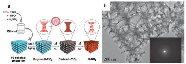
After the sol-gel process, a high-temperature treatment is always necessary for template removal and framework crystallization. Unlike amorphous silica framework with flexible Si--O--Si bond angle which can easily adapt to the curvature of mesopores, most metal oxides, on the other hand, tend to form relatively rigid crystalline phases with high lattice energies [66], therefore are more likely to suffer from framework collapse. To solve this problem, Lee et al. reported a combined assembly by soft and hard (CASH) templates by using poly(isoprene-block-ethylene oxide) (PI-b-PEO) as a structure-directing agent [67, 68]. When firstly calcined under an inert environment, PEO is easily decomposed on heating, whereas the more thermally stable PI, containing two sp2 carbons per monomer unit, is converted to a sturdy, amorphous carbon material to act as a rigid support to the mesostructured oxide wall. This in situ generated carbon residual is then removed by following heat treatment under oxidative atmosphere. In this way, highly crystalline mesoporous metal oxides can be obtained. Using diblock copolymer poly (ethylene oxide)-b-polystyrene (PEO-b-PS) as a structure directing agent, a highly ordered and crystallized mesoporous TiO2 material has been synthesized by Zhang et al. through ligand assisted and carbon-supported strategies as illustrated in Fig. 2 [63].

|
Download:
|
| Fig. 2. (a) The formation process of ordered mesoporous TiO2 with highly crystallized framework, (b) TEM image of mesoporous TiO2 from [100] direction, (c) HRTEM image of mesoporous TiO2, (d) FESEM image of products after calcination at 600 ℃ in N2, (e) FESEM image of products after calcination at 600 ℃ followed with 450 ℃ in air. Reprinted with permission [63]. Copyright 2011, John Wiley and Sons. | |
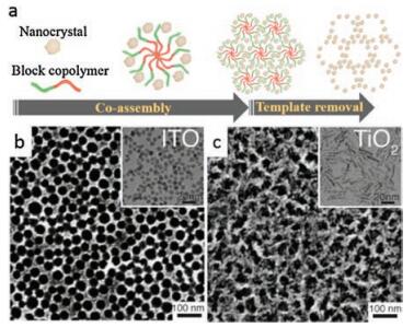
Another possible solution to mesostructure collapse is using pre-formed and fully crystallized nanocrystals to replace molecular metal precursors as the inorganic framework building blocks [37, 43, 69-74]. Typically, monodisperse crystalline metal oxide nanoparticles are first synthesized, and then co-assemble with block copolymers into mesostructured materials through an EISA process. Corma and co-workers [74] reported the synthesis of a hierarchically mesoporous material from monodisperse CeO2 nanoparticles and P123 triblock copolymers. The obtained mesostructure showed a well-defined hexagonal symmetry. The mesoporous CeO2 did not produce noticeable variations in the porosity even after the treatment at 700 ℃, indicating a remarkable thermal and hydrothermal stability. Except for CeO2, nanocrystals of other metal oxides including In2O3 [70], SnO2 [70], TiO2 [70], Mn3O4 [73], ZrO2 [71], and mixed oxides ITO [70], MnFe2O4 [73] etc. have also been used to co-assemble with structure directing agents, resulting in highly ordered mesostructures. The synthesis scheme is shown in Fig. 3.

|
Download:
|
| Fig. 3. (a) Schematic illustration of the synthesis of colloidal nanocrystal frameworks by EISA method. Top view FESEM images of (b) ITO nanocrystals mesoporous film and (c) TiO2 nanocrystals mesoporous film with inset of TEM images of ITO nanocrystals and TiO2 nanocrystals, respectively. (b) and (c) are Reprinted with permission [70]. Copyright 2012, American Chemical Society. | |
2.2. Hard templating synthesis (nanocasting)
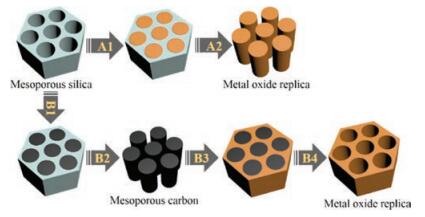
The soft templating method is not a universal way to fabricating ordered porous metal oxides since it fails in synthesizing many oxides of late transition metals [52]. As an alternative method, the "hard templating" method, or "nanocasting" as shown in Fig. 4, can be developed to synthesis porous metal oxides and other materials that are not available from soft templating method [75, 76]. In a typical nanocasting process, solid template is first synthesized and then impregnated with guest precursor, followed by heat treatment to convert the precursor compound into crystalline metal oxides. The crystalline metal oxides replica is then obtained after the removal of template matrix. A well-defined mesostructured WO3 replica from KIT-6 is shown in Fig. 5 [77].

|
Download:
|
| Fig. 4. Schematic illustration of hard-templating synthesis (nanocasting) strategy to fabricate mesoporous metal oxide replica. The synthesis pathway A directly uses mesoporous silica as the template matrix, where step A1 is the impregnation and crystallization of metal oxides, and step A2 is template removal. Pathway B includes mesoporous carbon as a transition template. B1: impregnation with carbon precursor and carbonization. B2: silica template removal. B3: impregnation and crystallization of metal oxides in carbon template. B4: carbon template removal. | |

|
Download:
|
| Fig. 5. (a, b) TEM images of the synthesized mesoporous WO3 replica from KIT-6 template via nanocasting, (c) HRTEM image of the ring structure with corresponding FFT in the inset. (d) The model of the uncoupled framework. Reprinted with permission [77]. Copyright 2007, John Wiley and Sons. | |
Ordered mesoporous silica synthesized via soft templating method has become the most commonly used hard template matrix due to its easily controlled synthesis and highly ordered mesostructure. Besides, ordered mesoporous carbon, directly synthesized or replicated from mesoporous silica, is an appropriate hard template for most oxides as well. Different mesostructured hard templates can be replicated into different mesostructured target materials [43, 76, 78]: Cylindrical pores structure (such as SBA-15) results in nanowire arrays, and spherical pores structure (such as KIT-6) results in nanosphere arrays [77]. Despite mesoporous template, colloidal crystal, such as polystyrene (PS) spheres [79], poly(methyl methacrylate) (PMMA) spheres [80], and silica spheres [81] can also act as hard template to fabricate ordered mesoporous or macroporous metal oxides. There is also another classification in which the "colloidal crystal templating method" is separated from hard templating method. Colloidal crystal templating is usually employed to fabricate 3-D macroporous networks like inverse opal [8, 82]. As indicated in Fig. 6 [82], the pre-formed closely packed spheres arrays act as the hard template matrix which is then immersed in a fluid precursor for deposition, followed by oxides crystallization and template removal. Mutil-components metal oxides can be obtained by impregnation with mixed metal precursors. It's worth mentioning that an ordered mesoporous-macroporous structure is available by using two different sized spheres or by the combination of colloidal crystal templating and surfactant as soft template [83]. The smaller sized spheres colloids or surfactant micelles can insert into the space between the larger colloidal spheres and form a hierarchical porous system. Zhang et al. [83] reported hierarchically ordered macro-/mesoporous TiO2 materials whose macropores generated from colloidal crystal PS spheres and the mesopores generated from triblock copolymer P123 (Fig. 7). The PS spheres arrays were impregnated with the titanium precursor solution containing P123, followed by an EISA process and calcination treatment for framework crystallization and templates removal.

|
Download:
|
| Fig. 6. (a) Schematic illustration of colloidal crystal templating method. (b, c) SEM images of the three-dimensional ordered macroporous ZnO/5% In. Reprinted with permission [82]. Copyright 2016, American Chemical Society. | |

|
Download:
|
| Fig. 7. (a) Schematic illustration of the synthesis process of hierarchically ordered macro-/mesoporous TiO2 films. (b) TEM of the macro-/mesoporous TiO2 after being calcined at 400 ℃. Two kinds of pores including mesopores and macropores can be observed from the TEM image.Reprinted with permission [83]. Copyright 2014, John Wiley and Sons. | |
The key issue for a successful nanocasting synthesis is to ensure that the metal species fulfill the pore channels of template matrix. Insufficient infiltration can result in an incompact metal oxides replica, and after the template removal, the incompact replica usually collapses into irregularly distributed metal oxides crystals eventually. It is noteworthy that even if the pores are completely filled with the precursor species, the subsequent conversion into metal oxides can unavoidably be accompanied with a volume shrinkage up to 90% [66, 84]. Therefore, it is necessary to repeat the precursor infiltration several times so as to fulfill the template matrix and obtain solid metal oxides replica. Take the simplest "wet impregnation" method [85] for example, by dispersing the (powdery) matrix in a dilute solution of the precursor, only a small amount of the solute species diffuses into the pores along with solvent and deposit in the channels [66]. Therefore, the impregnation process should be repeated more than once to get enough loading, but not too many times in case of the deposition at the out surface of the matrix. Many other infiltration methods are also available, such as "two solvents" method [86], melt method [87, 88], vapor-phase infiltration [89, 90], or supercritical fluids infiltration [91]. The next step is transformation of the precursor into crystalline metal oxides by thermal treatment. Materials templated from mesoporous silica can be directly calcined in air. For carbon or polymer templated synthesis, thermal treatment should be carried out in an inert atmosphere to avoid template combustion. The structure and morphology of oxide replicas can be affected by the calcination treatment: Sun et al. [84] reported that the size and shape of the container body in conjunction with the accessibility of the container opening can greatly influence the escape rate of water and other gas phase by-products of the calcination process, which in turn affects the nanocrystal growth of the materials inside the mesopore space of the template. The last step is template removal. The silica matrix can be etched either by basic KOH or NaOHsolution [92], or by HF solution [93], depending on the stability of the target metal oxides under the etching conditions. Considering the amphoteric properties of some oxides, such as ZnO which are not stable in both conditions, carbon or polymer templates should be used instead of silica templates [54, 94, 95]. Carbon or polymer templates are most easily removed by simple calcination in air.
Generally, the hard templating method can create metal oxides replicas with higher crystallinity than soft templating strategy. The support from hard templates prevents the structure collapse during heating treatment, therefore higher temperature or longer calcination is possible, resulting in higher crystallinity. However, considering the tedious synthesis procedures, the hard templating method is not a best solution in mass production.
3. Ordered porous structured metal oxides in gas sensingDifferent ordered porous metal oxides that have been applied to gas sensing are summarized in Table 1. The majority (approximately 90%) of sensing family are n-type metal oxides (e.g., SnO2, ZnO, In2O3, WO3 and Fe2O3, etc.) [96, 97] due to the excellent performance in sensing of reducing and flammable gases, therefore this section mainly focuses on the n-type semiconductors. A comprehensive introduction of p-type oxide (NiO, CuO, Cr2O3, Co3O4, and Mn3O4) sensors is available in another review [96].
|
|
Table 1 A comprehensive summary of the ordered porous metal oxides in gas sensing. |
3.1. Gas sensing mechanism
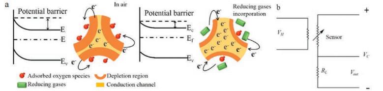
The gas sensing activity of metal oxides is based on the resistance change of the semiconductor when exposed in target gas. The resistance of the oxides may increase or decrease depending on both their physical nature and the gaseous analytes. The sensing mechanism of n-type semiconductors is illustrated in Fig. 8a. For n-type semiconductor whose current carrier is electrons (e-), under ambient atmosphere, oxygen molecules adsorb onto the surface of the oxides and "grab" electrons from the surface to form active species like O2- and O-, decreasing the electron density and increasing the oxide resistance [136]. The electron distribution of the oxides can only be affected within a limited depth from the surface by the adsorbed oxygen species.The affected region with low electron density is called the depletion layer, whose depth from the surface is called as Debye length (L), typically several nanometers[137]. The calculation of Debye length of semiconductor is given in Eq. (2)

|
Download:
|
| Fig. 8. (a) Sensing mechanism of n-type metal oxide semiconductors. The conduction area expands when exposed to reducing gases. (b) A typical electric circuit for gas sensing measurement. RL: load resistor; VC: the circuit voltage; Vout: output voltage. VH: heating voltage. | |

|
(2) |
where ε is the dielectric constant, kB is the Boltzmann's constant, T is the absolute temperature in Kelvins, q is the elementary charge, and Nd is the density of dopants (either donors or acceptors).
When n-type oxides are exposed in reducing gases such as CO, H2, CH4, ethanol, and acetone, electrons can be 'returned' back to depleted oxides through the surface reaction between adsorbed oxygen species and reducing gases, therefore the resistance of metal oxides decreases; while oxidizing analytes (Cl2, NOx, SO2, etc.) can intensify the electron depletion and cause an increasing of resistance. For p-type semiconductor whose current carrier is holes (h+), the resistance changes towards reducing gases and oxidizing gases is opposite to n-type oxides. In a resistive-type sensor, metal oxide sensing materials are deposited across two or more electrodes which measure the change in the electrical resistance of the oxides when exposed to target gases. A typical simplified electric circuit of gas sensing measurements is shown in Fig. 8b. The sensing material is electrically connected to the voltage dividing circuit including a certain load resistor connected in series. The resistance of sensing materials and its resistance change upon exposure to target gases can be calculated from the output voltage of load resistor. An appropriate load resistor (RL) whose resistance is comparable to the sensing material is needed to ensure the accuracy of calculation. Usually, the selection of RL is done manually in early types of measurement system. The recently developed measurement systems introduced an automatic switch of RL, which can greatly reduce the measurement errors and increase the potential for practical applications.
To evaluate the gas sensing performance of semiconductors, five parameters are employed: operating temperature, sensitivity, response-recovery time, selectivity and stability. The gas response (S) is usually defined as Ra/Rg, where Ra is the resistance in air and Rg is the resistance in target gas. The response time is usually defined as the time required for the variation in conductance to reach 90% of the equilibrium value starting from exposure to target gas, and the recovery time is the time required for the sensor to return to 10% above the original conductance in air after releasing the test gas, respectively.
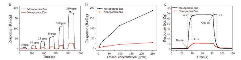
3.2. Porosity related properties in gas sensingGas sensing is a solid-gas interaction related process, thus the sensing properties are largely influenced by the specific surface area of solid metal oxides. Higher accessible surface area ratio ensures more adsorption and reaction sites, and therefore a larger resistance change and a better sensitivity. On the other hand, the pore size is also a key issue in gas sensing: large pores favor the gas diffusion but can cause a low surface area; while small pores always lead to a high surface area but are not sufficient pathway to allow analyte to diffuse within the oxide sensor layer. A comparison between ordered mesoporous ZnO (pore size ~29 nm) and none-mesoporous ZnO is shown in Fig. 9 [65]. The mesoporous structure not only increased the response toward ethanol but also shortened the response time from 11 s to 6 s, proving that gas diffusion is faster in mesoporous system. Tian et al. [138] synthesized a series of mesoporous SnO2 with different pore sizes ranging from 9.4 nm to 13.7 nm. It was found that the sample with larger pores, despite of lower surface area, exhibited higher sensitivity due to the good gas penetration in larger pores as shown in Fig. 10. However, in a regime of larger pore size, the increase of pore diameter could turn disadvantageous to sensitivity. For example, Xu et al. [129] synthesized three different macroporous rGO-SnO2 films using PS microspheres with different diameter (200 nm, 750 nm and 1000 nm) as the template, respectively, and they found that the film sensor templated from 200 nm PS microspheres exhibited the best sensitivity in detecting ethanol gas because of its higher surface area. Therefore, in order to achieve a good comprehensive sensing performance, a balance of pore size and surface area have to be found.

|
Download:
|
| Fig. 9. (a) Response – recovery curve. (b) Relationships between ethanol concentration and response of the mesoporous ZnO sensor and none-mesoporous ZnO sensor to ethanol vapors of different concentrations. (c) Dynamic response – recovery curve of the mesoporous ZnO and none-mesoporous ZnO to 50 ppm ethanol. Reprinted with permission [65]. Copyright 2015, Royal Society of Chemistry. | |

|
Download:
|
| Fig. 10. Structure model of (a, c) sample of 9.4 nm pore size and (b, d) sample of 13.7 nm pore size. Reprinted with permission [138]. Copyright 2013, Elsevier. | |
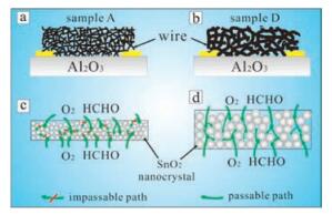
Besides the pore size and surface area, the pore structure can also influence the sensing performance. In this regard, two different crystalline mesoporous WO3 replicas have been synthesized by Rossinyol et al. [77] using SBA-15 (2D hexagonal mesostructure) and KIT-6 (3D cubic mesostructure) mesoporous silica as the hard templates, respectively. The KIT-6 replica showed a sponge like ordered mesoporous structure while the SBA-15 replica were prone to form aggregates and hence with poorer order degree. Under NO2 gas, the KIT-6 replica exhibited both a higher response and a faster response rate compared with the SBA-15 replica.
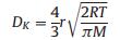
To better understand the gas diffusion in porous system, several diffusion model have been proposed [28, 30-33, 139-143]. In mesoporous systems, gas diffusion is marked by the fact that the dimensions of the pores are roughly comparable to the free mean paths of the gas molecules [28, 144, 145], and therefore, the surface diffusion, Knudsen diffusion and molecular diffusion take place in turn in this order as the pore size increases [33]. In the pore size range of 1–100 nm, gas diffusion is predominantly described by Knudsen diffusion as expressed in Eq. (3) [142], where the diffusion coefficient DK is linearly related to the pore width r; M is the molecular mass of the gas molecule; R and T are the universal gas constant and temperature, respectively. Apparently, larger pore size and smaller target gas molecule lead to faster gas diffusion. In other words, for larger pores (usually d > 50 nm), the mean free path (λ) of gas molecule is smaller than the pore size, which allows the target gas molecule to easily diffuse inside the framework; whereas in smaller pores, confinement of gas diffusion by the pore boundaries is significant. It should be mentioned that the mean free path of gas molecule is influenced by temperature and concentration, thus the comparable pore size to l is not necessarily 50 nm, but vary under different conditions.
|
(3) |
where the diffusion coefficient DK is linearly related to the pore width r; M is the molecular mass of the gas molecule; R and T are the universal gas constant and temperature, respectively.
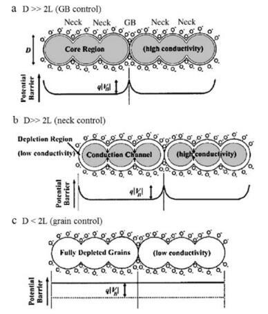
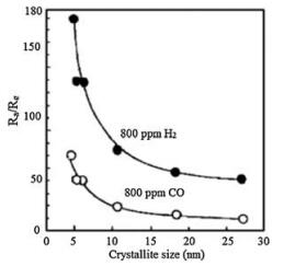
3.3. Framework nanostructureThe crystallinity of metal oxides is a fundamental requirement for gas sensing, and the grain size also plays an important role in resistance change [146-154]. As mentioned above, the electron density change only happens within the exterior layer of the oxide grains; therefore, the interior region inside of the depletion area have no contribution to the resistance change. In theory, grain sizes larger the twice the Debye length (L) are disadvantageous to the overall change in conductance of the material, as illustrated in Fig. 11 [155]. For large grains (D > > 2L), the highly conductive core region hardly participates in the discharge-recharge process when exposed to oxidizing gases and reducing gases, thus exhibiting poor response. For grains whose D value approaches but is still larger than 2L (D > 2L), a constricted channel forms by the depletion region that surrounds each neck, and consequently, the conductivity depends on both grain boundary barriers and the cross section area, therefore the sensitivity is enhanced and becomes grain size dependent. When D < 2L, the crystallites are almost fully depleted, implying that the whole grain participates in the charge transfer interactions with gas molecules. The energy bands of these interconnected grains are nearly flat, because no significant barriers for charge transfer exists in grain boundaries. Xu et al. [156] have studied the grain size effects of porous SnO2 sensor and found that, when the SnO2 crystallite size (D) is controlled in the range of 5–32 nm, the responses for H2, CO and i-C4H10 increase greatly as D decreases to be comparable with or less than 2L (~6 nm) (Fig. 12). It should be mentioned that, even though small crystallites could yield the highest sensitivity theoretically, the practical application of the ultrasmall metal oxide particles is limited due to the steeply decreased conductivity and unstable nature of the nanoparticles at high operating temperature.

|
Download:
|
| Fig. 11. Schematic model of the effect of the crystallite size on the sensitivity of metal-oxide gas sensors: (a) D >> 2L; (b) D > 2L; (c) D < 2L. Reprinted with permission [155]. Copyright 2004, AIP Publishing LLC. | |

|
Download:
|
| Fig. 12. The grain size effect on the responses of porous SnO2 under 800 ppm H2 or CO. Reprinted with permission [156]. Copyright 1991, Elsevier. | |
4. Strategy to improve sensing performance 4.1. Oxide heterojunctions
Among various semiconductive metal oxides, n-type oxides are more widely used than p-type ones, especially n-type SnO2, WO3, ZnO and In2O3 which have shown excellent performances in gas sensing. Some p-type oxides have also been used for gas sensing, such as NiO [44, 109, 151, 157, 158], Co3O4 [159, 160], CuO [22]. However, very few of them, either n-type or p-type oxides, can meet all of the sensing requirements (sensitivity, selectivity, response-recover speed and operating temperature) [97, 137]. To tackle this problem, exciting progress has been made on developing multi-composites metal oxides sensors which exhibit better sensing performances [161]. By definition, the combination of n-type oxides and p-type oxides is called "p-n junction", and the combination between two different n-type oxides is "n-n junction", and "p-p junction" between two different p-type oxides. At present, there is no one theory that can govern all heterostructured-gas interactions because of the diversity of structures and materials available.
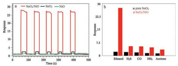
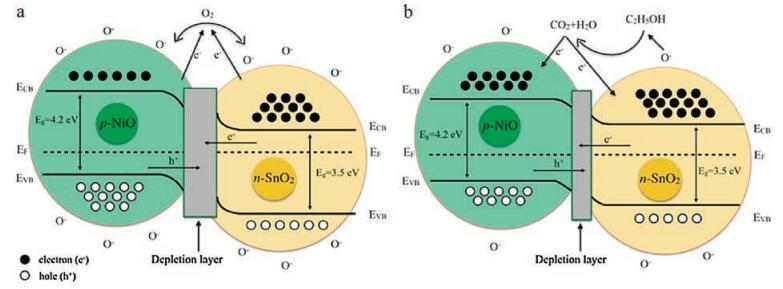
In a p-n junction, the electrons at high energy can transfer across the oxide interface to unoccupied low energy state to equalize the Fermi level, resulting in a 'band bending'. This energy transition can change the energy structure of both p-side and nside, and leading to a better sensitivity. Take the p-type NiO/n-type SnO2 heterojunctions [162] for example, the response of p-NiO/nSnO2 is higher than pristine SnO2 or NiO (Fig. 13). The possible explanation of band structure is shown in Fig. 14: Electrons transfer from SnO2 to NiO while holes from NiO to SnO2, until the Fermi level of the system is equalized, leading to an evenwider depletion region at the oxides interface and the increased resistance. When the sensor is exposed to reducing ethanol gas, C2H5OH molecules reacts with the adsorbed oxygen species and releases the electrons back to the bulk, increasing the conductivity of the materials. Moreover, ethanol also releases electrons into p-type NiO and cause the electron-hole recombination which decreases the concentration of holes. The decreasing holes in NiO results in the increase of electrons. Consequently, the concentration gradient of the same carriers on both sides of p-n heterojunction is decreased, therefore the diffusion of carriers is greatly reduced, and resulting in a thinner depletion layer at the interface, thus the resistance of the SnO2/NiO composites in ethanol can be further decreased. In general, compared with the pure SnO2 sensor, the formation of p-n heterojunction between SnO2 and NiO sensor greatly increases the resistance in air and decreases the resistance in C2H5 gas. This theoretical model can also be used to explain other materials systems of heterojunction, such as CuO/ZnO [8] and CuO/SnO2 [130].

|
Download:
|
| Fig. 13. (a) The response characteristic of pure SnO2 nanowebs and SnO2/NiO nanowebs sensors to 100ppm of ethanol at 300 ℃. (b) Responses of pure SnO2 nanowebs and SnO2/NiO nanowebs sensors to different gases with a concentration of 100ppm at 300 ℃. Reprinted with permission [162]. Copyright 2016, Elsevier. | |

|
Download:
|
| Fig. 14. Proposed band structure model for a p-NiO/n-SnO2 heterojunction when surrounded by (a) air, (b) ethanol gas. ECB, lower level of conduction band; EF, Fermi level; EVB, upper level of valence band. Reprinted with permission [162]. Copyright 2016, Elsevier. | |
Electron transfer also occurs in n-n or p-p heterojunctions due to the energy level differences between two different metal oxides [82, 163]. Charge can immigrate from the oxide of a higher Fermi energy to the lower one, increasing the energy barrier and hence resistance of composite, and can therefore facilitate the oxygen adsorption on the surface.
Except for energy band bending, some metal oxides can promote the surface catalytic decomposition of target gases. This process is most commonly described in the use of CuO composite materials in H2S detection [164, 165]. Specifically, H2S reacts with CuO nanoparticles and transforms them into CuS. The left-over hydrogen then "spills over" onto the surface of the host material and acts as a reducing agent, thus decreasing the resistance. In this way, the CuO phase helps to sensitize the host oxide to H2S analyte.
4.2. Modification by noble metalIn many gas sensing process, the conductivity change is determined by the efficiency of surface catalytic reactions between the analyte gas molecules and the adsorbed species [28, 97]. Therefore, the enhancement of catalytic activity on the material surface becomes a promising method to improve sensing performance. Finely dispersed clusters of noble metals such as Pt [131], Au [26, 157], Ag [166, 167] or Pd [168, 169] can (1) increase the sensitivity, (2) decrease the response time, and sometime (3) diminish the cross sensitivity to water, owing to the high-effective oxidation catalytic activity of the noble metals [18]. The noble metal clusters can be loaded onto the surface of the sensing oxides by various methods, such as wet impregnation, sputtering, and gas phase evaporation. As for the most widely used impregnation method, the semiconductive metal oxides is first synthesized and then immersed in a noble metal precursor solution (like HAuCl4 aqueous solution for Au deposition), followed by chemical reduction, or by deposition of the pre-formed clusters from a colloidal suspension.
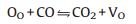
Two theories have been proposed to explain the enhancement of sensitivity by loading Pd on SnO2 which can be generalized to most noble metal and semiconductive oxides [97, 168]. One is "chemical mechanism" which suggests that the noble metal nanoparticles catalytically activate the gas molecules in various way. In this process, both vacancies repopulated by oxygen and the repopulation rate are increased, leading to a greater and faster electron depletion of the semiconductive oxides at a lower temperature than that for the pristine oxides. Morazzoni et al. [131] reported an enhancement of electrical response towards CO by doping Pt into SnO2 inverse opal thin films, and suggested the mechanism as the following equilibria:
|
(4.1) |
|
(4.2) |
|
(4.3) |
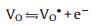
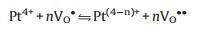
Where OO is the anion in a regular oxygen site, VO is neutral oxygen vacancy, VO· is singly ionized oxygen vacancy, and VO·· is doubly ionized oxygen vacancy (n=2, 4 for Pt). The change in oxidation state of noble metal centers, as described in reaction 4.3, shifts to the right to release electrons in reaction 4.2 and ultimately favors the production of VO defects (reaction 4.1), increasing the number of electrons injected into the conduction band with respect to undoped SnO2. It is expected that the easier the metal reduction, the easier the transfer of electrons to the conduction band, and the higher the noble metal oxidation state, the stronger the electrical response.
Another theory called "electronic mechanism" was also proposed to explain the enhancement of sensitivity by loading noble metal. The "electronic mechanism" proposes that the depleted area forms around the noble metal particles and improves the sensitivity to the modulation of the nano-Schottky barriers and thus the width of the conduction channel, due to the oxidation state changes of the noble metal accompanying oxygen adsorption and desorption [168].
5. Prospects and challengesThe tunability of the synthesis approaches and the widely available templates provide a great potential to prepare ordered porous metal oxides with various compositions and structures. The ordered porous structures including mesoporous or macroporous or/and their heretical combination greatly facilitate the gas diffusion that can thus increase both the sensitivity and response-recovery speed. The factors that affect sensing performances include the materials-related chemical composition, pore size, pore symmetry, film thickness, and operating temperature, humidity. Apart from the design of gas-diffusion-favored structure, other ways to improve the sensing performance of ordered porous oxides have been also studied, such as the formation of p-n or n-n heterojunctions, doping with noble metals, doping with carbon species, UV activation, oxygen vacancies generation and etc. Besides, the design and synthesis of asymmetric hybrid junctions with multi-functions, or/and the control of surface active sites and energy states can also creating possibilities in sensing properties. By varying these influential factors, it is believed that more and more high-performance materials can be synthesized for gas sensing.
However, there are still some practical issues that have to be considered. The most important one is the operating temperature. Metal oxide sensors are usually operated at a high temperature ranges from 150 ℃ to 400 ℃. Such high temperatures can lead to high power consumption, and sometime can even ignite flammable and explosive gases. Most importantly, working at high temperature can lead to further crystallization of metal oxide framework, leading to larger grain sizes. It can not only decrease the sensitivity but also lead to the structure collapse especially for small-pore-sized structures. The second issue is the film crack. During heat treatment for crystallization and removal of template, the sensing materials usually suffer a framework shrinkage of 10%-40%, which may cause cracks in the oxide film [101]. The cracks cut the film into isolate islands, leading to an extra high resistance and a lower stability. These nanostructure changes mentioned above bring about the last issue that is the long-term stability of the sensing devices. Semiconductor oxide sensors often exhibit a resistance drift after operating for a relatively long time. In addition to nanostructure changes, the losing of oxygen vacancies may also be a possible reason for resistance drift. Therefore, in order to lower the operating temperature and obtain a good longterm stability, it is necessary to explore new porous structures and develop new solutions to effectively activate metal oxides at low temperatures, and this will become the next trend of sensing materials development.
AcknowledgmentsThis work was supported by the National Natural Science Foundation of China (Nos. 51372041, 51422202, and 21673048), the "Shu Guang" Project (No. 13SG02) supported by Shanghai Municipal Education Commission and Shanghai Education Development Foundation, the National Youth Top-notch Talent Support Program in China, China Postdoctoral Science Foundation (No. KLH1615138), Shanghai Nature Science Foundation of China (Nos. 14ZR1416600 and 15ZR1402000), and Shanghai Pujiang Program, China (No. 16PJ1401100). The authors extend their appreciation to the International Scientific Partnership Program ISPP at King Saud University for funding this research work through ISPP# 0094.
| [1] |
J. Yick, B. Mukherjee, D. Ghosal, Comput. Netw. 52 (2008) 2292-2330. |
| [2] |
H. Akimoto, Science 302 (2013) 1716-1719. |
| [3] |
J.N. Anker, W.P. Hall, O. Lyandres, et al., Nat. Mater. 7 (2008) 442-453. DOI:10.1038/nmat2162 |
| [4] |
T.G. Drummond, M.G. Hill, J.K. Barton, Nat. Biotechnol. 21 (2003) 1192-1199. DOI:10.1038/nbt873 |
| [5] |
G. Wysocki, A.A. Kosterev, F.K. Tittel, Appl. Phys. B 80 (2005) 617-625. DOI:10.1007/s00340-005-1764-y |
| [6] |
J.N. Smith, A. Keil, J. Likens, et al., Analyst 135 (2010) 994-1003. DOI:10.1039/b921162d |
| [7] |
H. Li, F. Meng, J. Liu, et al., Sens. Actuators B 166- 167 (2012) 519-525. |
| [8] |
Y. Xie, R. Xing, Q. Li, et al., Sens. Actuators B 211 (2015) 255-262. DOI:10.1016/j.snb.2015.01.086 |
| [9] |
S. Shao, H. Wu, S. Wang, et al., J. Mater. Chem. C 3 (2015) 10819-10829. |
| [10] |
M. Righettoni, A. Tricoli, S.E. Pratsinis, Anal. Chem. 82 (2010) 3581-3587. DOI:10.1021/ac902695n |
| [11] |
T. Seiyama, A. Kato, K. Fujiishi, et al., Anal. Chem. 34 (1962) 1502-1503. DOI:10.1021/ac60191a001 |
| [12] |
T. Seiyama, S. Kagawa, Anal. Chem. 38 (1966) 1069-1073. |
| [13] |
X.J. Huang, Y.K. Choi, Sens. Actuators B 122 (2007) 659-671. DOI:10.1016/j.snb.2006.06.022 |
| [14] |
W. Kim, M. Choi, K. Yong, Sens. Actuators B 209 (2015) 989-996. DOI:10.1016/j.snb.2014.12.072 |
| [15] |
J.X. Wang, X.W. Sun, Y. Yang, et al., Nanotechnology 17 (2006) 4995-4998. DOI:10.1088/0957-4484/17/19/037 |
| [16] |
X.D. Wang, C.J. Summers, Z.L. Wang, Nano Lett. 4 (2004) 423-426. DOI:10.1021/nl035102c |
| [17] |
B. Cheng, J.M. Russell, W.S. Shi, et al., J. Am. Chem. Soc. 126 (2004) 5972-5973. DOI:10.1021/ja0493244 |
| [18] |
H.S. Woo, C.W. Na, J.H. Lee, Sensors 16 (2016) 1531. DOI:10.3390/s16091531 |
| [19] |
N. Ramgir, N. Datta, M. Kaur, et al., Colloids Surf. A 439 (2013) 101-116. DOI:10.1016/j.colsurfa.2013.02.029 |
| [20] |
Z.Y. Fan, D.W. Wang, P.C. Chang, et al., Appl. Phys. Lett. 85 (2004) 5923-5925. DOI:10.1063/1.1836870 |
| [21] |
E. Comini, G. Faglia, G. Sberveglieri, et al., Appl. Phys. Lett. 81 (2002) 1869-1871. DOI:10.1063/1.1504867 |
| [22] |
M.J. Song, S.W. Hwang, D. Whang, Talanta 80 (2010) 1648-1652. DOI:10.1016/j.talanta.2009.09.061 |
| [23] |
X.F. Pan, X. Liu, A. Bermak, et al., Acs Nano 7 (2013) 9318-9324. DOI:10.1021/nn4040074 |
| [24] |
M.A. Mahjoub, G. Monier, C. Robert-Goumet, et al., J. Phys. Chem. C 120 (2016) 11652-11662. DOI:10.1021/acs.jpcc.6b00135 |
| [25] |
S. Barth, F. Hernandez-Ramirez, J.D. Holmes, et al., Prog. Mater. Sci. 55 (2010) 563-627. DOI:10.1016/j.pmatsci.2010.02.001 |
| [26] |
E. Della Gaspera, A. Antonello, M. Guglielmi, et al., J. Mater. Chem. 21 (2011) 4293-4300. DOI:10.1039/c0jm03494k |
| [27] |
G. Wang, B. Dou, Z. Zhang, et al., J. Environ. Sci. 30 (2015) 65-73. DOI:10.1016/j.jes.2014.10.015 |
| [28] |
X. Wang, Y. Wang, F. Tian, et al., J. Phys. Chem. C 119 (2015) 15963-15976. |
| [29] |
B. Fruhberger, M. Grunze, D.J. Dwyer, Sens. Actuators B 31 (1996) 167-174. DOI:10.1016/0925-4005(96)80062-1 |
| [30] |
Z. Yang, Y. Huang, G. Chen, et al., Sens. Actuators B 140 (2009) 549-556. DOI:10.1016/j.snb.2009.04.052 |
| [31] |
X. Sun, H. Hao, H. Ji, et al., ACS Appl. Mater. Interfaces 6 (2014) 401-409. DOI:10.1021/am4044807 |
| [32] |
G. Inoue, K. Yokoyama, J. Ooyama, et al., J. Power Sources 327 (2016) 610-621. DOI:10.1016/j.jpowsour.2016.07.107 |
| [33] |
G. Sakai, N. Matsunaga, K. Shimanoe, et al., Sens. Actuators B 80 (2001) 125-131. DOI:10.1016/S0925-4005(01)00890-5 |
| [34] |
J.S. Beck, J.C. Vartuli, W.J. Roth, et al., J. Am. Chem. Soc. 114 (1992) 10834-10843. DOI:10.1021/ja00053a020 |
| [35] |
P.D. Yang, D.Y. Zhao, D.I. Margolese, et al., Chem. Mater. 11 (1999) 2813-2826. DOI:10.1021/cm990185c |
| [36] |
G.J.d.A.A. Soler-Illia, E.L. Crepaldi, D. Grosso, et al., Curr. Opin.Colloid Interface 8 (2003) 109-126. DOI:10.1016/S1359-0294(03)00002-5 |
| [37] |
B.A. Helms, T.E. Williams, R. Buonsanti, et al., Adv. Mater. 27 (2015) 5820-5829. DOI:10.1002/adma.v27.38 |
| [38] |
Y. Wan, H. Yang, D.Y. Zhao, Acc. Chem. Res. 39 (2006) 423-432. DOI:10.1021/ar050091a |
| [39] |
Y. Wang, J. Guo, T. Wang, et al., Nanomaterials 5 (2015) 1667-1689. DOI:10.3390/nano5041667 |
| [40] |
Y. Ren, Z. Ma, P.G. Bruce, Chem. Soc. Rev. 41 (2012) 4909-4927. DOI:10.1039/c2cs35086f |
| [41] |
Y. Shi, Y. Wan, D. Zhao, Chem. Soc. Rev. 40 (2011) 3854-3878. DOI:10.1039/c0cs00186d |
| [42] |
W. Li, D. Zhao, Chem. Commun. 49 (2013) 943-946. DOI:10.1039/C2CC36964H |
| [43] |
D. Gu, F. Schuth, Chem. Soc. Rev. 43 (2014) 313-344. DOI:10.1039/C3CS60155B |
| [44] |
D.Y. Zhao, Q.S. Huo, J.L. Feng, et al., J. Am. Chem. Soc. 120 (1998) 6024-6036. DOI:10.1021/ja974025i |
| [45] |
D. Zhao, J. Feng, Q. Huo, et al., Science 279 (1998) 548-552. DOI:10.1126/science.279.5350.548 |
| [46] |
A. Rumplecker, F. Kleitz, E.L. Salabas, et al., Chem. Mater. 19 (2007) 485-496. DOI:10.1021/cm0610635 |
| [47] |
Y. Shi, B. Guo, S.A. Corr, et al., Nano Lett. 9 (2009) 4215-4220. DOI:10.1021/nl902423a |
| [48] |
Q.S. Huo, D.I. Margolese, U. Ciesla, et al., Nature 368 (1994) 317-321. DOI:10.1038/368317a0 |
| [49] |
Q.S. Huo, D.I. Margolese, U. Ciesla, et al., Chem. Mater. 6 (1994) 1176-1191. DOI:10.1021/cm00044a016 |
| [50] |
P.D. Yang, D.Y. Zhao, D.I. Margolese, et al., Nature 396 (1998) 152-155. DOI:10.1038/24132 |
| [51] |
P.D. Yang, T. Deng, D.Y. Zhao, et al., Science 282 (1998) 2244-2246. DOI:10.1126/science.282.5397.2244 |
| [52] |
A.S. Poyraz, C.H. Kuo, S. Biswas, et al., Nat. Commun. 4 (2013) 2952. |
| [53] |
Y. Wan, Y. Shi, D. Zhao, Chem. Commun.(2007), 897-926. DOI:10.1039/b610570j |
| [54] |
T. Wagner, T. Waitz, J. Roggenbuck, et al., Thin Solid Films 515 (2007) 8360-8363. DOI:10.1016/j.tsf.2007.03.021 |
| [55] |
G. Soler-Illia, A. Louis, C. Sanchez, Chem. Mater. 14 (2002) 750-759. DOI:10.1021/cm011217a |
| [56] |
D. Grosso, C. Boissiere, B. Smarsly, et al., Nat. Mater. 3 (2004) 787-792. DOI:10.1038/nmat1206 |
| [57] |
D. Grosso, F. Cagnol, G.J.d.A.A. Soler-Illia, et al., Adv. Funct. Mater. 14 (2004) 309-322. DOI:10.1002/(ISSN)1616-3028 |
| [58] |
J. Fan, S.W. Boettcher, G.D. Stucky, Chem. Mater. 18 (2006) 6391-6396. DOI:10.1021/cm062359d |
| [59] |
U. Schubert, J. Mater. Chem. 15 (2005) 3701-3715. DOI:10.1039/b504269k |
| [60] |
Q. Li, J. Xu, Z. Wu, et al., Phys. Chem. Chem. Phys. 12 (2010) 10996-11003. DOI:10.1039/c004469e |
| [61] |
W. Luo, Y. Li, J. Dong, et al., Angew. Chem. Int. Ed. 52 (2013) 10505-10510. DOI:10.1002/anie.201303353 |
| [62] |
D. Feng, W. Luo, J. Zhang, et al., J. Mater. Chem. A 1 (2013) 1591-1599. DOI:10.1039/C2TA00588C |
| [63] |
J. Zhang, Y. Deng, D. Gu, et al., Adv. Enery Mater. 1 (2011) 241-248. DOI:10.1002/aenm.201000004 |
| [64] |
B. Eckhardt, E. Ortel, D. Bernsmeier, et al., Chem. Mater. 25 (2013) 2749-2758. DOI:10.1021/cm400535d |
| [65] |
X. Zhou, Y. Zhu, W. Luo, et al., J. Mater. Chem. A 4 (2016) 15064-15071. DOI:10.1039/C6TA05687C |
| [66] |
T. Wagner, S. Haffer, C. Weinberger, et al., Chem. Soc. Rev. 42 (2013) 4036-4053. DOI:10.1039/C2CS35379B |
| [67] |
J. Lee, M.C. Orilall, S.C. Warren, et al., Nat. Mater. 7 (2008) 222-228. DOI:10.1038/nmat2111 |
| [68] |
Y. Ye, C. Jo, I. Jeong, et al., Nanoscale 5 (2013) 4584-4605. DOI:10.1039/c3nr00176h |
| [69] |
P. Xu, X. Li, H. Yu, et al., Sensors 14 (2014) 19023-19056. DOI:10.3390/s141019023 |
| [70] |
R. Buonsanti, T.E. Pick, N. Krins, et al., Nano Lett. 12 (2012) 3872-3877. DOI:10.1021/nl302206s |
| [71] |
D.P. Song, C. Li, W. Li, et al., ACS Nano 10 (2016) 1216-1223. DOI:10.1021/acsnano.5b06525 |
| [72] |
J.B. Rivest, R. Buonsanti, T.E. Pick, et al., J. Am. Chem. Soc. 135 (2013) 7446-7449. DOI:10.1021/ja403071w |
| [73] |
I.E. Rauda, R. Buonsanti, L.C. Saldarriaga-Lopez, et al., ACS Nano 6 (2012) 6386-6399. DOI:10.1021/nn302789r |
| [74] |
A. Corma, P. Atienzar, H. Garcia, et al., Nat. Mater. 3 (2004) 394-397. DOI:10.1038/nmat1129 |
| [75] |
A.H. Lu, F. Schueth, Adv. Mater. 18 (2006) 1793-1805. DOI:10.1002/(ISSN)1521-4095 |
| [76] |
H.F. Yang, D.Y. Zhao, J. Mater. Chem. 15 (2005) 1217-1231. |
| [77] |
E. Rossinyol, A. Prim, E. Pellicer, et al., Adv. Funct. Mater. 17 (2007) 1801-1806. DOI:10.1002/(ISSN)1616-3028 |
| [78] |
M. Hartmann, Chem. Mater. 17 (2005) 4577-4593. DOI:10.1021/cm0485658 |
| [79] |
B.T. Holland, C.F. Blanford, T. Do, et al., Chem. Mater. 11 (1999) 795-805. DOI:10.1021/cm980666g |
| [80] |
Y. Xia, B. Gates, Y. Yin, et al., Adv. Mater. 12 (2000) 693-713. DOI:10.1002/(ISSN)1521-4095 |
| [81] |
X. Zheng, Y. Lv, Q. Kuang, et al., Chem. Mater. 26 (2014) 5700-5709. DOI:10.1021/cm5025475 |
| [82] |
Z. Wang, Z. Tian, D. Han, et al., ACS Appl. Mater. Interfaces 8 (2016) 5466-5474. DOI:10.1021/acsami.6b00339 |
| [83] |
R. Zhang, D. Shen, M. Xu, et al., Adv. Enery Mater. 4 (2014) 1301725. DOI:10.1002/aenm.201301725 |
| [84] |
X. Sun, Y. Shi, P. Zhang, et al., J. Am. Chem. Soc. 133 (2011) 14542-14545. DOI:10.1021/ja2060512 |
| [85] |
S.P. Jiang, Mat. Sci. Eng. A Struct. 418 (2006) 199-210. DOI:10.1016/j.msea.2005.11.052 |
| [86] |
K. Jiao, B. Zhang, B. Yue, et al., Chem. Commun.(2005), 5618-5620. |
| [87] |
Y.M. Wang, Z.Y. Wu, H.J. Wang, et al., Adv. Funct. Mater. 16 (2006) 2374-2386. DOI:10.1002/(ISSN)1616-3028 |
| [88] |
W. Yue, W. Zhou, J. Mater. Chem. 17 (2007) 4947-4952. DOI:10.1039/b709076e |
| [89] |
N. Nishiyama, M. Yamaguchi, Y. Nishiyama, et al., J. Non-Cryst. Solids 351 (2005) 3218-3224. DOI:10.1016/j.jnoncrysol.2005.08.012 |
| [90] |
B. Gong, Q. Peng, J.S. Jur, et al., Chem. Mater. 23 (2011) 3476-3485. DOI:10.1021/cm200694w |
| [91] |
T.A. Crowley, K.J. Ziegler, D.M. Lyons, et al., Chem. Mater. 15 (2003) 3518-3522. DOI:10.1021/cm034139v |
| [92] |
H. Tüysüz, Y.J. Hwang, S.B. Khan, et al., Nano Res. 6 (2012) 47-54. |
| [93] |
Y. Shi, C. Hua, B. Li, et al., Adv. Funct. Mater. 23 (2013) 1832-1838. DOI:10.1002/adfm.v23.14 |
| [94] |
A. Chernikov, S. Horst, T. Waitz, et al., J. Phys. Chem. C 115 (2011) 1375-1379. DOI:10.1021/jp104293e |
| [95] |
A.H. Lu, W. Schmidt, A. Taguchi, et al., Angew. Chem. Int. Ed. 41 (2002) 3489-3492. DOI:10.1002/1521-3773(20020916)41:18<3489::AID-ANIE3489>3.0.CO;2-M |
| [96] |
H.J. Kim, J.H. Lee, Sens. Actuators B 192 (2014) 607-627. DOI:10.1016/j.snb.2013.11.005 |
| [97] |
C. Wang, L. Yin, L. Zhang, et al., Sensors 10 (2010) 2088-2106. DOI:10.3390/s100302088 |
| [98] |
N. Van Quy, T.M. Hung, T.Q. Thong, et al., Curr. Appl. Phys. 13 (2013) 1581-1588. DOI:10.1016/j.cap.2013.06.002 |
| [99] |
R. Lu, W. Zhou, K. Shi, et al., Nanoscale 5 (2013) 8569-8576. DOI:10.1039/c3nr01903a |
| [100] |
S. Shao, M. Dimitrov, N. Guan, et al., J. Mater. Chem. 19 (2009) 8411. DOI:10.1039/b908238g |
| [101] |
T.J. Ha, M.H. Hong, C.S. Park, et al., Sens. Actuators B 181 (2013) 874-879. DOI:10.1016/j.snb.2013.02.093 |
| [102] |
Y. Li, W. Luo, N. Qin, et al., Angew. Chem. Int. Ed. 53 (2014) 9035-9040. DOI:10.1002/anie.201403817 |
| [103] |
S. Shao, X. Qiu, D. He, et al., Nanoscale 3 (2011) 4283-4289. DOI:10.1039/c1nr10678c |
| [104] |
T. Wagner, C.-D. Kohl, M. Froba, et al., Sensors 6 (2006) 318-323. DOI:10.3390/s6040318 |
| [105] |
A. Stanoiu, S. Somacescu, J.M. Calderon-Moreno, et al., Sens. Actuatuors B 231 (2016) 166-174. DOI:10.1016/j.snb.2016.02.137 |
| [106] |
Y. Ren, X. Zhou, W. Luo, et al., Chem. Mater. 28 (2016) 7997-8005. DOI:10.1021/acs.chemmater.6b03733 |
| [107] |
S. Shao, R. Koehn, H. Wu, et al., New J. Chem. 40 (2016) 5523-5530. DOI:10.1039/C5NJ03463A |
| [108] |
Q. Liu, W.M. Zhang, Z.M. Cui, et al., Microporous Mesoporous Mater. 100 (2007) 233-240. DOI:10.1016/j.micromeso.2006.10.041 |
| [109] |
X. Lai, G. Shen, P. Xue, et al., Nanoscale 7 (2015) 4005-4012. DOI:10.1039/C4NR05772D |
| [110] |
P. Xue, X. Yang, X. Lai, et al., Sci. Bull. 60 (2015) 1348-1354. DOI:10.1007/s11434-015-0852-6 |
| [111] |
V.K. Tomer, S. Duhan, J. Mater. Chem. A 4 (2016) 1033-1043. DOI:10.1039/C5TA08336B |
| [112] |
X. Sun, X. Hu, Y. Wang, et al., J. Phys. Chem. C 119 (2015) 3228-3237. DOI:10.1021/jp5124585 |
| [113] |
X. Liu, R. Wang, T. Zhang, et al., Sens. Actuators B 150 (2010) 442-448. DOI:10.1016/j.snb.2010.05.033 |
| [114] |
Y. Qin, F. Wang, W. Shen, et al., J. Alloys Compd. 540 (2012) 21-26. DOI:10.1016/j.jallcom.2012.06.058 |
| [115] |
Q. Gao, W.T. Zheng, C.D. Wei, et al., J. Nanomater. 2013 (2013) 1-7. |
| [116] |
C.Y. Liu, C.F. Chen, J.P. Leu, J. Electrochem. Soc. 156 (2009). |
| [117] |
T. Waitz, T. Wagner, T. Sauerwald, et al., Adv. Funct. Mater. 19 (2009) 653-661. DOI:10.1002/adfm.v19:4 |
| [118] |
S. Vetter, S. Haffer, T. Wagner, et al., Sens. Actuators B 206 (2015) 133-138. DOI:10.1016/j.snb.2014.09.025 |
| [119] |
D. Klaus, D. Klawinski, S. Amrehn, et al., Sens. Actuators B 217 (2015) 181-185. DOI:10.1016/j.snb.2014.09.021 |
| [120] |
T. Wagner, C.D. Kohl, C. Malagù, et al., Sens. Actuators B 187 (2013) 488-494. DOI:10.1016/j.snb.2013.02.025 |
| [121] |
T. Wagner, C.D. Kohl, S. Morandi, et al., Chemistry 18 (2012) 8216-8223. DOI:10.1002/chem.v18.26 |
| [122] |
J. Zhao, W. Wang, Y. Liu, et al., Sens. Actuators B 160 (2011) 604-608. DOI:10.1016/j.snb.2011.08.035 |
| [123] |
J.H. Smått, M. Lindén, T. Wagner, et al., Sens. Actuators B 155 (2011) 483-488. DOI:10.1016/j.snb.2010.12.051 |
| [124] |
T. Waitz, B. Becker, T. Wagner, et al., Sens. Actuators B 150 (2010) 788-793. DOI:10.1016/j.snb.2010.08.001 |
| [125] |
J. Tu, N. Li, X. Lai, et al., Appl. Surf. Sci. 256 (2010) 5051-5055. DOI:10.1016/j.apsusc.2010.03.055 |
| [126] |
S.A. Ghom, C. Zamani, S. Nazarpour, et al., Sens. Actuators B 140 (2009) 216-221. DOI:10.1016/j.snb.2009.02.078 |
| [127] |
E. Rossinyol, A. Prim, E. Pellicer, et al., Sens. Actuators B 126 (2007) 18-23. DOI:10.1016/j.snb.2006.10.017 |
| [128] |
A. Prim, E. Pellicer, E. Rossinyol, et al., Adv. Funct. Mater. 17 (2007) 2957-2963. DOI:10.1002/(ISSN)1616-3028 |
| [129] |
S. Xu, F. Sun, Z. Pan, et al., ACS Appl. Mater. Interfaces 8 (2016) 3428-3437. DOI:10.1021/acsami.5b11607 |
| [130] |
S. Zhang, P. Zhang, Y. Wang, et al., ACS Appl. Mater. Interfaces 6 (2014) 14975-14980. DOI:10.1021/am502671s |
| [131] |
M. D'Arienzo, L. Armelao, A. Cacciamani, et al., Chem. Mater. 22 (2010) 4083-4089. DOI:10.1021/cm100866g |
| [132] |
B. Zhang, W. Fu, H. Li, et al., Appl. Surf. Sci. 363 (2016) 560-565. DOI:10.1016/j.apsusc.2015.12.042 |
| [133] |
L. Xu, Z. Dai, G. Duan, et al., Sci. Rep. 5 (2015) 10507. DOI:10.1038/srep10507 |
| [134] |
B. Wang, F. Liu, X. Yang, et al., ACS Appl. Mater. Interfaces 8 (2016) 16752-16760. DOI:10.1021/acsami.6b04219 |
| [135] |
L. Jia, W. Cai, Adv. Funct. Mater. 20 (2010) 3765-3773. DOI:10.1002/adfm.201001216 |
| [136] |
N. Barsan, U. Weimar, J. Electroceram. 7 (2001) 143-167. DOI:10.1023/A:1014405811371 |
| [137] |
N. Yamazoe, G. Sakai, K. Shimanoe, Catal. Surv. Asia 7 (2003) 63-75. DOI:10.1023/A:1023436725457 |
| [138] |
S. Tian, X. Ding, D. Zeng, et al., Sens. Actuators B 186 (2013) 640-647. DOI:10.1016/j.snb.2013.06.073 |
| [139] |
S.I. Garcés-Polo, J. Villarroel-Rocha, K. Sapag, et al., Chem. Eng. J. 302 (2016) 278-286. DOI:10.1016/j.cej.2016.05.057 |
| [140] |
N. Matsunaga, G. Sakai, K. Shimanoe, et al., Sens. Actuators B 83 (2002) 216-221. DOI:10.1016/S0925-4005(01)01043-7 |
| [141] |
G. Inoue, M. Kawase, J. Power Sources 327 (2016) 1-10. DOI:10.1016/j.jpowsour.2016.07.037 |
| [142] |
N. Matsunaga, G. Sakai, K. Shimanoe, et al., Sens. Actuators B 96 (2003) 226-233. DOI:10.1016/S0925-4005(03)00529-X |
| [143] |
H.M. Alsyouri, J.Y.S. Lin, J. Phys. Chem. B 109 (2005) 13623-13629. DOI:10.1021/jp0509764 |
| [144] |
S. Mitani, K. Sakai, K. Takagi, Jpn. Appl. Phys. 39 (2000) 146-149. |
| [145] |
G.L. Aranovich, M.D. Donohue, Phys. A 373 (2007) 119-141. DOI:10.1016/j.physa.2006.05.056 |
| [146] |
A. Katoch, G.J. Sun, S.W. Choi, et al., Sens. Actuators B 185 (2013) 411-416. DOI:10.1016/j.snb.2013.05.030 |
| [147] |
A. Katoch, Z.U. Abideen, J.H. Kim, et al., Met. Mater. Int. 22 (2016) 942-946. DOI:10.1007/s12540-016-6099-1 |
| [148] |
A. Tamvakos, D. Calestani, D. Tamvakos, et al., Microchim. Acta 182 (2015) 1991-1999. DOI:10.1007/s00604-015-1539-z |
| [149] |
G. Korotcenkov, S.D. Han, B.K. Cho, et al., Crit. Rev. Solid State 34 (2009) 1-17. DOI:10.1080/10408430902815725 |
| [150] |
B. Lyson-Sypien, M. Radecka, M. Rekas, et al., Sens. Actuators B 211 (2015) 67-76. DOI:10.1016/j.snb.2015.01.050 |
| [151] |
J.M. Choi, J.H. Byun, S.S. Kim, Sens. Actuators B 227 (2016) 149-156. DOI:10.1016/j.snb.2015.12.014 |
| [152] |
J. Liu, G. Jin, Z. Zhai, et al., Electron. Mater. Lett. 11 (2015) 457-465. DOI:10.1007/s13391-015-4399-0 |
| [153] |
M. Tiemann, Chemistry 13 (2007) 8376-8388. DOI:10.1002/(ISSN)1521-3765 |
| [154] |
T. Kida, S. Fujiyama, K. Suematsu, et al., J. Phys. Chem. C 117 (2013) 17574-17582. DOI:10.1021/jp4045226 |
| [155] |
A. Rothschild, Y. Komem, J. Appl. Phys. 95 (2004) 6374-6380. DOI:10.1063/1.1728314 |
| [156] |
C.N. Xu, J. Tamaki, N. Miura, et al., Sens. Actuators B 3 (1991) 147-155. DOI:10.1016/0925-4005(91)80207-Z |
| [157] |
G. Mattei, P. Mazzoldi, M.L. Post, et al., Adv. Mater. 19 (2007) 561-564. DOI:10.1002/(ISSN)1521-4095 |
| [158] |
J.A. Dirksen, K. Duval, T.A. Ring, Sens. Actuators B 80 (2001) 106-115. DOI:10.1016/S0925-4005(01)00898-X |
| [159] |
G. Zhang, L. Dang, L. Li, et al., Cryst. Eng. Comm. 15 (2013) 4730-4738. DOI:10.1039/c3ce40206a |
| [160] |
J.M. Xu, J.P. Cheng, J. Alloys Compd. 686 (2016) 753-768. DOI:10.1016/j.jallcom.2016.06.086 |
| [161] |
D.R. Miller, S.A. Akbar, P.A. Morris, Sens. Actuators B 204 (2014) 250-272. DOI:10.1016/j.snb.2014.07.074 |
| [162] |
Y. Wang, H. Zhang, X. Sun, Appl. Surf. Sci. 389 (2016) 514-520. DOI:10.1016/j.apsusc.2016.07.073 |
| [163] |
L. Wang, J. Li, Y. Wang, et al., Sci. Rep. 6 (2016) 35079. DOI:10.1038/srep35079 |
| [164] |
F. Shao, M.W.G. Hoffmann, J.D. Prades, et al., Sens. Actuators B 181 (2013) 130-135. DOI:10.1016/j.snb.2013.01.067 |
| [165] |
A. Chowdhuri, V. Gupta, K. Sreenivas, et al., Appl. Phys. Lett. 84 (2004) 1180-1182. DOI:10.1063/1.1646760 |
| [166] |
G. Zhu, Y. Liu, H. Xu, et al., Cryst. Eng. Comm. 14 (2012) 719-725. DOI:10.1039/C1CE06041D |
| [167] |
Y. Wang, X. Cui, Q. Yang, et al., Sens. Actuators B 225 (2016) 544-552. DOI:10.1016/j.snb.2015.11.065 |
| [168] |
A. Kolmakov, D.O. Klenov, Y. Lilach, et al., Nano Lett. 5 (2005) 667-673. DOI:10.1021/nl050082v |
| [169] |
Y. Shen, T. Yamazaki, Z. Liu, et al., Thin Solid Films 517 (2009) 6119-6123. DOI:10.1016/j.tsf.2009.05.036 |