 2018, Vol. 29


Plasmonic sensing is rooted in the light-matter interaction and applied in fundamental science as well as practical technologies. Plasmonic nanostructures can confine light through localized surface plasmon resonance (LSPR), thereby enabling a series of novel plasmonic techniques. LSPR has become a merging hot spot in the fields of nanophotoelectron and nanotechnology. One of the most important applications of this phenomenon is plasmonic sensing, which takes the advantage of strong LSPR absorption bands and enhanced local electromagnetic field (EF), owning to the excitation of charge density oscillations by light. On one hand, LSPR sensing is more suitable to measure the short-range changes in vicinity of the plasmonic nanostructures than the commercial propagating surface plasmon resonance sensing [1]. On the other hand, plasmonic sensing based on LSPR possesses the advantages of high sensitive, label-free and real-time measurements. Compared with other sensitive sensing assays [2-4], such as enzyme linked immunosorbent assay [5], electrochemical assay [6] and chemiluminescence assay [7] those need labels with specific chemical elements, electrochemiluminescent assay [8] and photo-luminescent assay [9] that can provide high sensitivity and in various environments, LSPR biosensing holds great potential to be developed into highly sensitive, ease-of-use, highly miniaturized and wearable devices in simple optical paths such as transmission-mode and reflection-mode. In the past several decades, there have been achievements of exquisite size- and shape- control in the fabrication of noble metal nanostructures (i.e., gold, silver and platinum), as well as their extensive applications in biological and chemical sensing [10-12]. For example, our previous work reported a type of gold nano-mushroom arrays (GNMA) that possess a figure of merit reaching ~108, which is comparable to the theoretically predicted upper limit for standard propagating surface plasmon resonance sensors; we also applied the antibody-modified GNMA with good anti-interference ability to the rapid detection of alpha-fetoprotein, which is an important biomarker specific to hepatocellular carcinoma in clinical patient serum [4, 11, 13]. However, the LSPR sensing based on noble metal is still restricted in scientific researches, due to the limitations of their intrinsic properties (Interband transitions of gold-based LSPR are supposed to cause a dissipative channel at wavelengths below 550 nm. Silver-based nanostructures are extremely vulnerable to color degradation resulting from oxidation and sulfidation [14, 15]), high prime price and high process cost. In addition, the LSPR bands of noble metal materials mostly locate in the visible region and only some exquisitely designed ones can exhibit strong absorption in the near-infrared region, while the plasmonic nanostructures with LSPR bands in the ultraviolet (UV), mid-infrared (MIR) and far-infrared are also in demand, such as the in-vivo biosensing [16]. Thereby, researchers have started to look for other novel materials for plasmonic sensing, such as non-noble metal and semiconductor materials, especially the ones holding attractive properties including low cost, high stability, easy fabrication, appropriate locations and narrow peaks of LSPR bands. As an overview in recent years, non-noble-metal material plasmonics are experiencing an increasing development in both fundamental researches and ondemand biosensing applications towards low-cost and high-performance. Herein, we review the research progress of nonnoble-metal materials with nanostructures for plasmonic biosensing. The physical and sensing principles of LSPR sensors are briefly introduced at first; then non-noble-metal materials, such as copper, aluminum, graphene, semiconductor and other materials for plasmonic sensing are summarized. After that, a rational discussion about the future prospective of novel materials for plasmonic sensing is given.
2. Principle of LSPR sensingLSPR arises from the light-matter interaction. As for plasmonic nanostructures, surface plasmons are confined to a small region quite close to the nanostructures. A resonance will happen when the frequency of the extra incident EF matches the natural frequency of surface plasmons, which is known as LSPR [17, 18].
LSPR is mainly responsible for two effects: (ⅰ) the enhancement of local EF around the nanostructures, and (ⅱ) the peaks of the plasmonic nanosubstrate's extinction spectra. First, the local EF can be intensively enhanced, which is the foundation of several surface-enhanced techniques such as surface enhance Raman scattering and surface enhanced fluorescence. This enhanced EF is greatest at the interface and falls off with the distance. The efficient distance of this surface enhancement is termed as "decay length" or "evanescent field" [19]. Second, there will be a maximum in the nanosubstrate's extinction spectra caused by the light-plasmon resonance. The peaks are determined by the dielectric properties both of the plasmonic nanosubstrate and the external environment. The shape of the extinction spectra can be affected by the environment within the decay length, which lays the foundation of LSPR sensing [11].
We take spherical nanoparticles as a typical example of LSPR sensing substrates [1, 18]. The remarkable Mie's theory gave us the equation of a nanosphere's extinction spectra:

|
(1) |
where ε1 and 1d refer to the real and imaginary part of the complex dielectric constant, respectively; εm is the dielectric constant of the media adjacent to the nanospheres; V is the volume of a nanosphere.
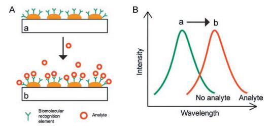
When the dielectric properties of the local environment are changed by the adsorption of analytes, there will be a peak-wavelength shift observed in the extinction spectra (Fig. 1). Since the refractive index (RI) is related to the dielectric properties, LSPR sensors can detect the RI changes in the local environment caused by the adsorption of analytes. The relationship between the peak-wavelength shift (△λmax) and the RI change (△n) is shown as follows:

|
Download:
|
| Fig. 1. LSPR biosensing principle. (A) Biomolecular recognition elements (e.g., antibody) on the surface of metal nanosubstrate (a) recognize and capture analyte (e.g., antigen) present in a liquid sample (b), producing a local increase in the refractive index at the metal surface. (B) The increase of local refractive index induces a peak-wavelength shift of the extinction spectra | |

|
(2) |
where m represents the sensitivity factor of the nanosubstrate (in nm per refractive index unit, nm/RIU); △n represents the RI changes near the metallic surface; d is the distance be εm tween the binding analyte and the surface; 1d is the decay length of the enhanced EF [19]. The RI sensing principle of LSPR substrates is shown by Eq. (2) and illustrated by Fig. 1.
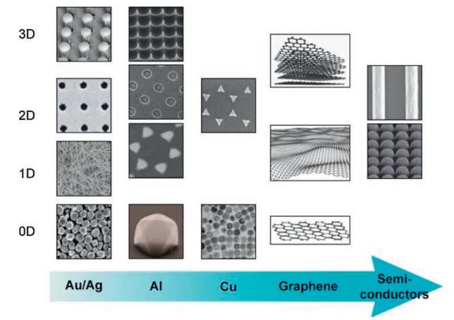
3. MaterialsLSPR generation is theoretically possible in any metal, alloy or semiconductor with a large negative real dielectric constant and small positive imaginary part of the dielectric constant. The vast majority of LSPR sensing experiments have been carried out on gold or silver [20]. Gold is preferred for biological application in many literatures, because of its chemical inert nature, resistance to oxidation, biocompatibility, and thiol-gold association that has been well developed for immobilization of biomolecules. Silver is a popular material for LSPR at visible frequencies due to the narrow plasmon line width, which is ascribed to its intrinsic optical properties. However, silver is easily oxidised under ordinary laboratory condition. Besides, the intrinsic property of the materials, nanostructures can also tailor LSPR bands in the extinction spectra. Therefore, the choices of materials and the designs of nanostructures are the core issues for fabricating a LSPR sensing substrate with desirable optical properties, and the nonnoble-metal materials with lower cost and good or better optical properties are attractive in the field of plasmonic sensing [15]. Various plasmonic sensing nanosubstrates in different dimensions are presented in Fig. 2. Except Au and Ag, non-noble-metal materials such as Cu, Al, semiconductor and graphene have already been studied and utilized for plasmonic biosensing, and these materials will be categorized and discussed according to their properties and applications in this review, respectively.

|
Download:
|
| Fig. 2. Plasmonic materials with different shapes and sizes for biosensing. Reprinted with permission [11, 13, 15, 27, 33, 37-40]. Copyright 2015, the Royal Society of Chemistry. Copyright 2013, Nature Publishing Group. Copyright 2013, 2017, WILEY-VCH Verlag GmbH & Co. KGaA, Weinheim. Copyright 2007, 2008, 2015, 2017, American Chemical Society. Copyright 2016, Elsevier B.V. | |
3.1. Cu
Copper (Cu) possesses a large negative real and a small imaginary of the dielectric complex, and in theory it is capable of supporting plasmon resonances in the visible-near infrared (vis-NIR) region, which is similar with the noble metals [21-24]. Besides, Cu is earth-abundant compared with noble metals and thus is appealing as a low-cost plasmonic material for LSPR sensing. However, the stability of Cu is compromised due to its corrosion in aqueous solutions and oxidation in ambient laboratory atmosphere at room temperature [24, 25]. The LSPR of the Cu nanostructures is unstable and significantly affected by the presence of oxides, such as Cu2O and CuO. Therefore, the corrosion and oxidation of Cu-based plasmonic nanostructures are the core problems to be solved in the field of Cu-based plasmonic biosensing [26].
Several strategies have been used to overcome the problems associated with the corrosion and surface oxidation of Cu nanostructures. The first approach is to remove oxides away from the Cu nanostructures by removal agents. Chan et al. have proven that removing the copper oxides with glacial acetic acid and protecting the Cu nanostructures in N2 environment can bring a sharp and intense LSPR peak of the Cu nanoparticles, which is comparable to the LSPR peaks of Ag and Au [27]. In the second approach, reducing agents (e.g., N2H4, ascorbic acid and hydrazine hydrate) can also be used to slow down the formation of oxides during the synthesis of Cu nanostructures [25, 28]. The third method is to apply stabilizers in chemical synthesis, such as polyvinyl alcohol, polyvinyl pyrolidone and starch [29-31]. Susman et al. have reported that the corrosion inhibitor benzotriazole can be adsorbed onto the surface of Cu nanoparticles, and then effectively stabilizes the optical features of the nanosubstrates. In this way, a stable and reliable determination of the RI sensitivity of their Cu-based LSPR nanosubstrates was achieved [32]. In addition, Crane et al. have encapsulated SiO2 onto trioctyl-n-phosphine (TOP)-capped Cu nanoparticles, and yielded an aqueous Cu-SiO2 core-shell suspension with stable and well-preserved LSPR properties of the Cu cores [33].
Cu-based LSPR biosensors have been developed for the detection of gas and biomolecules. Ghodselahi et al. fabricated a LSPR sensing substrate of Cu@CuO core-shell nanoparticles (NPs) hexagonal arrays for sensing CO by measuring the absorbance spectra [34]. X-ray photoelectron spectroscopy indicated that the CO molecule was physically absorbed on the surface of the Cu-based LSPR nanosubstrates, and this adsorption of CO caused not only the intensity changes but also the peak-wavelength shifts of the LSPR nanosubstrate's absorbance spectra. An average shift of 10-2 nm per molecule absorption can be observed, which indicated the single-molecular detection of CO on the Cu-based LSPR nanosubstrates. Kim et al. have fabricated a multiplex sensing chip by using Cu-capped silica nanoparticle arrays as LSPR sensing substrates [35]. This optical LSPR biosensor was designed for multiplex sensing of target DNAs. Target DNAs were applied to specific spots on the sensing chip. The LSPR peak shifts of each spot were measured after the hybridization of target DNAs with the probes on the specific spot and this Cu-based LSPR biosensing chip displayed a detection limit of 10 fmol/L (50 zmol) of DNAs (Fig. 3).

|
Download:
|
| Fig. 3. (A) Schematic of the multiplex sensing chip based on Cu-capped silica nanoparticle arrays for the detection of DNAs. The LSPR peak shifts of each spot on the sensing chip was expressed in color (B and C) and represented by the bar size on the panels (D and E), respectively. The deionized water without target DNAs was applied to the sensing chip as a negative control. Abbreviations: Vvu, V. vulnificus; Sal, Salmonella spp.; Sau, S. aureus; Sep, S. epidermidis; Efa, E. faecalis; Kox, K. oxytoca; Ngo, N. gonorrhea. Reprinted with permission [35]. Copyright 2011, American Chemical Society. | |
3.2. Al
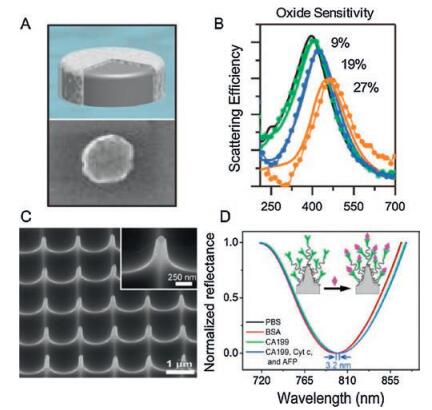
As an overview in recent years, aluminum (Al) plasmonics are experiencing an increasing development in both fundamental researches and on-demand biosensing applications towards low-cost and high-performance [36-39]. For one thing, Al exhibits attractive properties including low cost, high natural abundance, and ease of processing by a wide variety of methods such as complementary metal oxide semiconductor (CMOS) process. For another, Al plasmonics enable tunable plasmon resonances across the broad UV-vis-NIR region of the spectrum, which takes an advantage over the relatively narrow vis-NIR plasmon resonance region of noble metal materials [40]. Knight et al. observed that the energy of the Al-nanodisk LSPR is determined by the percentage of oxide present on the surface of Al (Figs. 4A and B) [41]. This understanding paves the way toward the use of Al as a low-cost plasmonic material with properties and potential biosensing applications similar to those of noble metals.

|
Download:
|
| Fig. 4. (A) An isolated Al nanodisk with a 3 nm surface oxide. (B) Scattering spectra of 100 nm diameter Al nanodisks with varying metal oxide fractions (9% (green), 19% (blue), and 27% (orange)). (C) The side view of the Al nanopyramid arrays (NPA) The inset in is a magnification image of a typical Al nanopyramid. (D) Representative reflectance spectra for detecting CA199 on the anti-CA199 modified Al nanopyramid by specific interaction. A and B were reprinted with permission [41]. Copyright 2014, American Chemical Society. C and D were reprinted with permission [40]. Copyright 2016, Elsevier B.V. | |
Norek et al. explored the possibility of biosensing using UV plasmon of the Al nanoconcave arrays fabricated by electrochemical anodization [42]. Though the surface plasmons theory predicted the sensitivity of the nanoconcave array up to 423 nm/RIU, the experimental ones which were estimated by immersing the substrate into various solvents presented lower sensitivities, due to the appearance of the short range SPR and wide LSPR band. It is obvious that the UV plasmonic sensitivity of Al nanoconcave array needs to be largely improved for on-demand ultrasensitive biosensing. Barrios et al. reported Al nanohole arrays with a RI sensitivity of 487 nm/RIU for label-free biosensing [43]. The nanohole arrays were fabricated through electron beam lithography (EBL) and treated with oxygen-gas plasmon, producing an oxide protecting layer that is more resistant to corrosion and pitting than native oxide, which perhaps claims for the improvement of Al nanosubstrates. Our group fabricated a kind of Al nanopyramid arrays (NPA) with a high sensitivity of 819 nm/RIU, which was even comparable with that of noble metal materials (Figs. 4C and D) [40]. The Al NPA was prepared through a two-step procedure consisting of denting and subsequent electrochemical etching. We have further demonstrated the Al NPA as a biosensor for one-step detecting cytochrome c (Cyt c) and carbohydrate antigen 199 (CA199), and the limits of detection were determined to be 800 nmol/L and 29 ng/mL, respectively.
3.3. SemiconductorSemiconductors are another potential materials for plasmonic biosensing, due to the ease of fabrication and flexibility of tuning their properties such as carrier concentration [20]. Heavily doped semiconductors can exhibit a negative dielectric constant under the incident light in IR frequencies [44]. So heavily doped semiconductor with large bandgap and high carrier mobility can serve as a low-loss plasmonic material for plasmonic biosensing in the IR region [20]. The LSPR peaks of semiconductors mainly depend on the density of free charge carriers, the charge carrier effective mass and geometric factors. In comparison to metals with fixed charge carrier density, the density of free charge carriers of heavily doped semiconductors can vary with changes of doping degree or even with changes of surface ligands, leading to the change of LSPR peaks [45]. However, it is still quite challenging to achieve doping levels high enough to bring the crossover frequency of semiconductors into the visible range [44].
One of the most popular semiconductors in the field of optoelectronics is metal oxide, which has been widely studied. Indium tin oxide (ITO) is a prototypical transparent conductive oxide (TCO) material, which consists of 90 wt% metal oxide semiconductor In2O3, doped with a group Ⅳ element Sn. The surface plasmon polaritions in ITO have been demonstrated between 1.8 μm and 1.9 μm, therefore ITO appears to be a potential plasmonic material in the IR region [46]. Since ITO is a non-stoichiometric compound, its optical properties largely depend on the growth/deposition processes and annealing conditions. The ITO LSPR peaks can be tuned from 1618 nm to ~2200 nm by controlling the Sn concentration [47]. Beside ITO, zinc oxides with high-performance conductivity such as aluminum-zinc-oxide (AZO) and gallium-zinc-oxide (GZO) and Ⅲ-V semiconductors (e.g., GaAs, GaN, GaP) can also be promising alternative plasmonic materials for biosensing in the IR region.
Another group of doped semiconductor materials is mainly copper-deficient copper chalcogenide nanocrystals (NCs), including copper sulfide (Cu2-xS), copper selenide (Cu2-xSe) and copper telluride (Cu2-xTe). The LSPR prosperities of Cu2-xS NCs in the IR region were first observed and identified in 2009, presuming that the free charges in Cu2-xS NCs are free holes associated with cation vacancies [48]. The LSPR peaks can shift to higher frequencies with the increase of copper deficiency. Guo et al. built a highly sensitive LSPR biosensor based on glutathione capped Cu2-xS NCs for the analysis of heavy metal ion Pb2+ in water [49]. The detection limit of Pb2+ was estimated to be 0.25 mmol/L (or 52.5 ppb), which is comparable to that conducted by metal-based LSPR nanostructures and fluorescence-based assays using quantum dots.
3.4. GrapheneGraphene is a two-dimension (2D) form of carbon atoms arranged in a honeycomb lattice, which has already displayed a wide range of extraordinary mechanical, electric, magnetic and thermal properties with a multitude of exciting applications [50-52]. The electronic band structure of intrinsic graphene can be described as a semiconductor with a vanishing band gap or a metal with a vanishing Fermi surface, leading to the high electron density and the mobility of graphene [53]. The electric gating leads to a dramatic change in optical properties of graphene because of its impact on the strong interband transitions [54], which makes surface plasmons on graphene similar to those on metal/dielectric interfaces. Therefore, graphene is an attractive material as an alternative for noble metals in the field of plasmonic biosensing.
Plasmonic materials such as noble metals mostly experience enormous losses in the frequency regimes of interest, while it has been demonstrated that surface plasmons in graphene experience lower losses compared to conventional metal/dielectric interfaces [55]. In contrast to noble metals, the plasmon resonance frequency of graphene can be tunable in the IR and terahertz region [55-57]. Furthermore, the EF of graphene surface plasmons display unprecedented spatial confinement, making graphene extremely attractive for enhanced light-matter interactions and integrated mid-IR photonics including plasmonic biosensing [58].
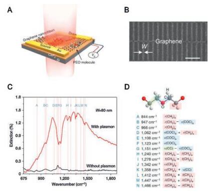
The IR range of graphene LSPR is particularly suited for biosensing, since this range covers the molecular vibration frequencies of biomolecules such as proteins, lipids, and DNA [59, 60]. Ju et al. reported that plasmon resonances in graphene can be controlled in structure-engineered graphene micro-ribbon arrays [56]. Graphene is found to exhibit an intense LSPR absorbance in the terahertz region at room temperature. Rodrigo et al. demonstrated a graphene-based LSPR biosensor with potentials for the quantitative detection of proteins and specific molecular identification [61]. The binding of IgG antibodies onto the sensing surface was proven to be obviously detectable in mid-IR within 15 nm from the graphene-based LSPR sensing surface. Hu et al. developed a graphene-based surface enhanced biosensor for the molecular fingerprint detection, which based on LSPR nanosubstrates of graphene plasmonic nano-structures on a 300-nm CaF2 thin-film (graphene/CaF2) [62]. This design of graphene-based LSPR nanosubstrates can avoid the plasmon-phonon hybridization and enable the first electrically tunable plasmon that covers the entire molecular fingerprint region for molecular detection with extremely high sensitivity down to sub-monolayer level. Highly sensitive and selective molecular fingerprinting was presented with a graphene plasmon based far-field Fourier transform infrared spectroscopy. The vibrational signature of ~8-nm polyethylene oxide (PEO) film was enhanced up by more than 20-fold (Fig. 5).

|
Download:
|
| Fig. 5. Graphene-based surface enhanced biosensor for molecular fingerprint detection. (A) Schematic of the biosensor. The graphene nanoribbon structure was designed on a CaF2 dielectric substrate (300 nm thick). The graphene plasmon resonance excited by the incident infrared beam (the red shaded pillar) can be tuned in situ by electrostatic doping through the gate voltage (Vg). (B) A scanning electron microscope image of the graphene nanoribbon pattern. Ribbon width (W): 80 nm. Width-to-pitch ratio: 1:3. Scale bar: 1 mm. (C) A comparison of the sensing results for an 8-nm-thick polyethylene oxide (PEO) film with (red curve) and without (black curve) graphene surface plasmon enhancement. The corresponding Fermi level is ~0.2 eV. The red vertical lines indicate various PEO molecular vibrational modes. (D) The list of PEO vibrational modes in the molecular fingerprint region and their positions in (C). The green, blue and red backgrounds represent the C—C, C—O—C, and methylene groups, respectively. The prefixes r, t, x and t indicate rocking, stretching, wagging and twisting modes, respectively. The suffixes s and a imply symmetric and anti-symmetric modes, respectively, with respect to the two-fold axis perpendicular to the helix axis and passing through the oxygen atom or center of the C—C bond. The + and -signs denote the phase relationship for the potential energy distribution of the coupled coordinates. Reprinted with permission [62]. Copyright 2016, Nature Publishing Group. | |
3.5. Others (composite)
Many materials such as intermetallics and ceramics exhibit plasmonic behaviors in the optical range. By introducing non-metallic elements into metal lattice, the carrier concentration could reduce, thus decreasing the excessive optical losses. Plasmonic intermetallic or metallic compounds possess many advantages such as optical tunability, ease of fabrication and integration, which could out-weigh the disadvantages of single material. Metal silicides and germanides, ceramics such as carbides, borides and nitrides, were all found to exhibit negative real permittivities in different parts of the optical spectrum [63]. Many of silicides exhibit metallic optical properties spanning the MIR and NIR range. Some silicides such as TiSi2 possess the high calculated quality factors for LSPR applications [64]. Besides, some materials such as titanium nitride (TiN), despite high-loss energy, have optical properties similar to gold [65].
Apart for these metal-nonmetal compounds, many intermetallics such as binary compounds of noble metals and transition metals, noble-alkali compounds could also provide metallic optical properties [64]. For example, a binary metal nitride system such as TixZr1-xN might exhibit better optical properties than TiN and ZrN. However, none of these materials possesses all the desirable properties, and exhibits low optical losses. There is a great promise in optimizing the properties of these materials. The important development towards the design of better plasmonic materials could come from the theoretical domain.
4. Conclusions and perspectivesIn conclusion, we reviewed the non-noble-metal materials for plasmonic sensing by the types of materials and their applications in biosensing. Moreover, the plasmonic properties of Cu, Al, semiconductors, graphene and other materials have been systematically presented. Cu and Al are both plasmonic materials with attractive properties including low cost and high abundance. Specially, the plasmonic resonances of Al are across the broad UV-vis-NIR region of the spectrum, which is the only metal material exhibiting LSPR resonance peak in the UV region of the spectrum. However, the oxidization issues during the fabrication processes of both Al and Cu-based plasmonic nanostructures are the core problems to be solved. Semiconductors are considered as potential alternative plasmonic materials since they are easy to be processed and integrated into micro-devices. Their plasmonic resonances mainly locate in the IR region and vary with the degree of doping. However, the doping mechanism is complicated and it is still quite challenging to achieve doping levels high enough to bring the crossover frequency of semiconductors into the visible range. Graphene is a low-loss 2D plasmonic material, and its LSPR is tunable in the IR and terahertz region, which crosses the spectrum range covering the molecular vibration frequencies of biomolecules. However, the application of graphene still faces the challenge of high price and difficulty for mass production at present.
Above all, a final choice of plasmonic materials requires a balance between quality factor, fabrication practicality and cost. Compared to conventional noble materials such as gold and silver, these materials possess the properties of low cost, tunable plasmon resonances in UV and IR regions, and CMOS compatibility, which are important requirements of new plasmonic sensing material. The future trends of these materials for plasmonic biosensing lie in: (1) Developing new plasmonic materials, such as organic conjugated semiconductors. Organic nanostructured films based on conjugated small molecular semiconductors (SMSs) offer unique advantages over their inorganic and macromolecular counterparts including structural versatility, facile and highly controllable synthesis and film fabrication, and fine-tuning of optoelectronic properties. Yilmaz et al. recently reported that metal-free α, ω-diperfluorohexylquaterthiophene (DFH-4T) films showed unprecedented Raman EFs (>103) via a resonance chargetransfer mechanism between the DFH-4T substrate and the analyte [66]. This type of organic conjugated semiconductors presents a great potential and could bring a new very promising entry to develop as new plasmonic materials. (2) Exploring composites of metals and semiconductors for plasmonic sensing. It is clear to see that no single plasmonic material offers superior performance for all applications in a given wavelength range. Rather, a variety of material combinations must be fine-tuned and optimized for individual situations or applications. For example, the graphenedoping metal nanosubstrates (e.g., graphene/Au-nanoantennas [67], graphene/CaF2 [62], graphene/Pt3Ni [68]) combine the electron-phonon advantage of both plasmonic material such as low energy loss and highly tunable plasmonic resonances, and represent a new type of hybrid material that shows great promise for plasmonic sensing applications. (3) Controllable nanofabrication of novel plasmonic material such as graphene and semi-conductors, and explorations of the optical properties of these materials in UV and IR regions. Integrating these materials into complex plasmonic and metamaterial geometries is the key for plasmonic sensing devices, since the plasmonic property of the materials strongly depends on the nanostructures, deposition, and patterning. In addition, we could realize plasmonic and metamaterial devices with alternative plasmonic materials for improved performance and new functionalities. Alternative plasmonic materials enable to exploration of new physics such as negative refraction materials, epsilon-near-zero (ENZ) structures, high-performance hyperbolic metamaterials (HMMs) devices, and non-linear plasmonic devices. Overall, these non-noblemetal plasmonic materials are of great potential to be excellent alternatives to noble metals in the field of biosensing, which could be applied in the next-generation of practical sensing platform.
AcknowledgmentsThis work was supported by the National Natural Science Foundation of China (Nos. 21405183 and 21775168), the special support plan for training high-level talents in Guangdong Province (No. 2014TQ01R695), and the Fundamental Research Funds for the Central Universities (Nos.16lgjc62, 16lgjc85). The work was also supported in part by the Australia-China Joint Institute for Health Technology and Innovation.
| [1] |
K.M. Mayer, J.H. Hafner, Chem. Rev. 111(2011) 3828-3857. DOI:10.1021/cr100313v |
| [2] |
X. Yang, Y. Yu, Z. Gao, ACS Nano 8(2014) 4902-4907. DOI:10.1021/nn5008786 |
| [3] |
A.J. Haes, L. Chang, W.L. Klein, R.P. Van Duyne, J. Am. Chem. Soc. 127(2005) 2264-2271. DOI:10.1021/ja044087q |
| [4] |
W. Li, X. Jiang, J. Xue, Z. Zhou, J. Zhou, Biosens. Bioelectron. 68(2015) 468-474. DOI:10.1016/j.bios.2015.01.033 |
| [5] |
H. Ju, G. Yan, F. Chen, H. Chen, Electroanalysis 11(1999) 124-128. DOI:10.1002/(ISSN)1521-4109 |
| [6] |
H. Su, R. Yuan, Y. Chai, L. Mao, Y. Zhuo, Biosens. Bioelectron. 26(2011) 4601-4604. DOI:10.1016/j.bios.2011.04.043 |
| [7] |
C. Wang, J. Wu, C. Zong, J. Xu, H.X. Ju, Chin. J. Anal. Chem. 40(2012) 3-10. DOI:10.1016/S1872-2040(11)60518-5 |
| [8] |
Z.X. Zhou, Q.W. Shang, Y.F. Shen, et al., Anal. Chem. 88(2016) 6004-6010. DOI:10.1021/acs.analchem.6b01062 |
| [9] |
Z.X. Zhou, Y.F. Shen, Y. Li, et al., ACS Nano 9(2015) 12480-12487. DOI:10.1021/acsnano.5b05924 |
| [10] |
H. Chen, X. Kou, Z. Yang, W. Ni, J. Wang, Langmuir 24(2008) 5233-5237. DOI:10.1021/la800305j |
| [11] |
W. Li, L. Zhang, J. Zhou, H. Wu, J. Phys. Chem. C 3(2015) 6479-6492. |
| [12] |
K. Wang, S.G. Li, Y.J. Liu, et al., Anal. Chem. 89(2017) 7262-7268. DOI:10.1021/acs.analchem.7b01882 |
| [13] |
Y. Shen, J. Zhou, T. Liu, et al., Nat. Commun. 4(2013) 2381. |
| [14] |
S.J. Tan, L. Zhang, D. Zhu, et al., Nano Lett. 14(2014) 4023-4029. DOI:10.1021/nl501460x |
| [15] |
G.V. Naik, V.M. Shalaev, A. Boltasseva, Adv. Mater. 25(2013) 3264-3294. DOI:10.1002/adma.v25.24 |
| [16] |
J.E. Park, M. Kim, J.H. Hwang, J.M. Nam, Small Methods 1(2017) 1600032. DOI:10.1002/smtd.v1.3 |
| [17] |
J. Langer, S.M. Novikov, L.M. Liz-Marzan, Nanotechnology 26(2015) 322001. DOI:10.1088/0957-4484/26/32/322001 |
| [18] |
M.E. Stewart, C.R. Anderton, L.B. Thompson, et al., Chem. Rev. 108(2008) 494-521. DOI:10.1021/cr068126n |
| [19] |
J.N. Anker, W.P. Hall, O. Lyandres, et al., Nat. Mater. 7(2008) 442-453. DOI:10.1038/nmat2162 |
| [20] |
P.R. West, S. Ishii, G.V. Naik, et al., Laser Photonics Rev. 4(2010) 795-808. DOI:10.1002/lpor.v4:6 |
| [21] |
U. Kreibig, M. Vollmer, Optical Properties of Metal Clusters[M]. Berlin, Heidelberg: Springer, 1995.
|
| [22] |
C.F. Bohren, D.R. Huffman, Absorption and Scattering of Light by Small Particles[M]. New York: John Wiley & Sons, 1983.
|
| [23] |
E.J. Zeman, G.C. Schatz, J. Phys. Chem. 91(1987) 634-643. DOI:10.1021/j100287a028 |
| [24] |
D.B. Pedersen, S. Wang, S.H. Liang, J. Phys. Chem. C 112(2008) 8819-8826. DOI:10.1021/jp710619r |
| [25] |
I. Platzman, R. Brener, A.H. Haick, R. Tannenbaum, J. Phys. Chem. C 112(2008) 1101. DOI:10.1021/jp076981k |
| [26] |
G.V. Hartland, G. Schatz, J. Phys. Chem. C 115(2011) 15121-15123. DOI:10.1021/jp206376f |
| [27] |
G.H. Chan, J. Zhao, E.M. Hicks, G.C. Schatz, R.P. Van Duyne, Nano Lett. 7(2007) 1947-1952. DOI:10.1021/nl070648a |
| [28] |
F. Meng, S. Jin, Nano Lett. 12(2012) 234-239. DOI:10.1021/nl203385u |
| [29] |
Y. Lee, J.R. Choi, K.J. Lee, N.E. Stott, D. Kim, Nanotechnology 19(2008) 415604. DOI:10.1088/0957-4484/19/41/415604 |
| [30] |
S. Jeong, K. Woo, D. Kim, et al., Adv. Funct. Mater. 18(2008) 679-686. DOI:10.1002/(ISSN)1616-3028 |
| [31] |
M. Singh, I. Sinha, M. Premkumar, A.K. Singh, R.K. Mandal, Colloids Surf. A 359(2010) 88-94. DOI:10.1016/j.colsurfa.2010.01.069 |
| [32] |
M.D. Susman, Y. Feldman, A. Vaskevich, I. Rubinstein, Chem. Mater. 24(2012) 2501-2508. DOI:10.1021/cm300699f |
| [33] |
C.C. Crane, F. Wang, J. Li, et al., J. Phys. Chem. C 121(2017) 5684-5692. DOI:10.1021/acs.jpcc.6b11891 |
| [34] |
T. Ghodselahi, H. Zahrabi, M.H. Saani, M.A. Vesaghi, J. Phys. Chem. C 115(2011) 22126-22130. DOI:10.1021/jp204020j |
| [35] |
D.K. Kim, S.M. Yoo, T.J. Park, et al., Anal. Chem. 83(2011) 6215-6222. DOI:10.1021/ac2007762 |
| [36] |
W. Li, K. Ren, J. Zhou, Trend. Anal. Chem. 80(2016) 486-494. DOI:10.1016/j.trac.2015.08.013 |
| [37] |
M.J. McClain, A.E. Schlather, E. Ringe, et al., Nano Lett. 15(2015) 2751-2755. DOI:10.1021/acs.nanolett.5b00614 |
| [38] |
G.H. Chan, J. Zhao, G.C. Schatz, R.P. Van Duyne, J. Phys. Chem. C 112(2008) 13958-13963. DOI:10.1021/jp804088z |
| [39] |
Z.Q. Wei, Z.K. Zhou, Q.Y. Li, et al., Small 13(2017) 1700109. DOI:10.1002/smll.v13.27 |
| [40] |
W. Li, Y. Qiu, L. Zhang, et al., Biosens. Bioelectron. 79(2016) 500-507. DOI:10.1016/j.bios.2015.12.038 |
| [41] |
M.W. Knight, N.S. King, L. Liu, et al., ACS Nano 8(2014) 834-840. DOI:10.1021/nn405495q |
| [42] |
M. Norek, M. Włodarski, P. Matysik, Curr. Appl. Phys. 14(2014) 1514. DOI:10.1016/j.cap.2014.09.002 |
| [43] |
C.A. Barrios, V. Canalejastejero, S. Herranz, et al., Biosensors 5(2015) 417-431. DOI:10.3390/bios5030417 |
| [44] |
A.J. Hoffman, L. Alekseyev, S.S. Howard, et al., Nat. Mater. 6(2007) 946-950. DOI:10.1038/nmat2033 |
| [45] |
X. Liu, M.T. Swihart, Chem. Soc. Rev. 43(2014) 3908-3920. DOI:10.1039/C3CS60417A |
| [46] |
S. Franzen, J. Phys. Chem. C 112(2008) 6027-6032. DOI:10.1021/jp7097813 |
| [47] |
M. Kanehara, H. Koike, T. Yoshinaga, T. Teranishi, J. Am. Chem. Soc. 131(2009) 17736-17737. DOI:10.1021/ja9064415 |
| [48] |
Y. Zhao, H. Pan, Y. Lou, et al., J. Am. Chem. Soc. 131(2009) 4253-4261. DOI:10.1021/ja805655b |
| [49] |
M. Guo, W. C. Law, X. Liu, et al., Plasmonics 9(2014) 893-898. DOI:10.1007/s11468-014-9694-3 |
| [50] |
K.S. Novoselov, A.K. Geim, S.V. Morozov, et al., Science 306(2004) 666-669. DOI:10.1126/science.1102896 |
| [51] |
K.S. Novoselov, A.K. Geim, S.V. Morozov, et al., Nature 438(2005) 197-200. DOI:10.1038/nature04233 |
| [52] |
A.K. Geim, K.S. Novoselov, Nat. Mater. 6(2007) 183-191. DOI:10.1038/nmat1849 |
| [53] |
C. Tao, L. Jiao, O.V. Yazyev, et al., Nat. Phys. 7(2011) 616-620. DOI:10.1038/nphys1991 |
| [54] |
F. Wang, Y. Zhang, C. Tian, et al., Science 320(2008) 206-209. DOI:10.1126/science.1152793 |
| [55] |
M. Jablan, H. Buljan, M. Soljacic, Phys. Rev. B 80(2009) 245435. DOI:10.1103/PhysRevB.80.245435 |
| [56] |
L. Ju, B. Geng, J. Horng, et al., Nat. Nanotechnol. 6(2011) 630-634. DOI:10.1038/nnano.2011.146 |
| [57] |
A. Woessner, M.B. Lundeberg, Y. Gao, et al., Nat. Mater. 14(2015) 421-425. DOI:10.1038/nmat4169 |
| [58] |
B. Vasic, G. Isic, R. Gajic, J. Appl. Phys. 113(2013) 013110. DOI:10.1063/1.4773474 |
| [59] |
P.R. Griffiths, J.A.D. Haseth, Fourier Transform Infrared Spectrometry[M]. New York: Wiley, 2007.
|
| [60] |
T. Wenger, G. Viola, J. Kinaret, M. Fogelstrom, P. Tassin, 2D Mater. 4(2017), doi: http://dx.doi.org/10.1088/2053-1583/aa70ff.
|
| [61] |
D. Rodrigo, O. Limaj, D. Janner, H. Altug, et al., Science 349(2015) 165-168. DOI:10.1126/science.aab2051 |
| [62] |
H. Hu, X. Yang, F. Zhai, et al., Nat. Commun. 7(2016) 12334. DOI:10.1038/ncomms12334 |
| [63] |
G.V. Naik, J. Kim, A. Boltasseva, Opt. Mater. Express 1(2011) 1090-1099. DOI:10.1364/OME.1.001090 |
| [64] |
M.G. Blaber, M.D. Arnold, M.J. Ford, J. Phys.:Condens. Matter 22(2010) 143201. DOI:10.1088/0953-8984/22/14/143201 |
| [65] |
U. Guler, G.V. Naik, A. Boltasseva, V.M. Shalaev, A.V. Kildishev, Appl. Phys. B:Lasers Opt. 107(2012) 285-291. DOI:10.1007/s00340-012-4955-3 |
| [66] |
M. Yilmaz, E. Babur, O. Mehmet, et al., Nat. Mater. (2017), doi: http://dx.doi.org/10.1038/nmat4957.
|
| [67] |
Z.Y. Fang, Y.M. Wang, Z. Liu, et al., ACS Nano 6(2012) 10222-10228. DOI:10.1021/nn304028b |
| [68] |
A. Politano, G. Chiarello, 2D Mater. 4(2017), doi: http://dx.doi.org/10.1088/2053-1583/aa78c2.
|