 2017, Vol. 28


 ,
Zongbo Zhangc,
Caihong Xuc,
Wenfeng Qiub,
Liqiang Lib
,
Zongbo Zhangc,
Caihong Xuc,
Wenfeng Qiub,
Liqiang Lib
b Advanced Nano-materials Division, Key Laboratory of Nano-Devices and Applications, Suzhou Institute of Nano-Tech and Nano-Bionics, Chinese Academy of Sciences, Suzhou 215123, China;
c Laboratory of High-Tech Materials, Institute of Chemistry, Chinese Academy of Sciences, Beijing 100190, China
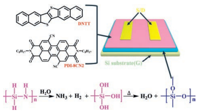
In recent years, organic thin-film transistors (OTFTs) have been attracting more and more attention in new generation electronic devices because of its great potential in a variety of applications such as flexible display, e-skin, radio frequency tag and so on [1-3]. Solution processing is one of highly promising ways to embody the advantages of OTFT such as low cost, large-area coverage, and high throughout [4-6]. Dielectric layer, one of the most vital parts of OTFTs, plays an important role in the performance of transistors that generally consists of inorganic materials and organic materials [1, 2, 7]. Inorganic materials such as silicon dioxide, silicon nitride and tantalum pentoxide are outstanding for their high dielectric constant and low leakage. Among these materials, the use of silicon dioxide as dielectric layer is particularly prevalent due to its excellent electrical properties and mature craftsmanship [8-11], moreover, its high dielectric strength and high breakdown voltage which is also suitable for high voltage integrated circuits [3, 12, 13].
There are many kinds of preparation methods, for example, thermal growth method, magnetron sputtering method and plasma enhanced chemical vapor deposition (PECVD) method [14-16]. Thermal growth method refers to a process that silicon surface was oxidized with a certain proportion of wet oxygen and dry oxygen under high temperature conditions. Thermal growth method is one of most commonly used methods because the equipment is cheap and the process is simple [17, 18]. However, thermal growth must use dry oxygen-wet oxygen-dry oxygen oxidation method which is difficult to operate and the preparation temperature is very high (> 800 ℃) [14, 19-21]. In addition, many extra steps have to be done if you want to control the growth rate in order to get ultra-thin silicon dioxide layer [14, 22]. Magnetron sputtering is a kind of physical vapor deposition (PVD) method which is repeatable and thickness adjustable to produce SiO2 thin film with high density and less pinholes [15, 23]. While moving ahead with Radio Frequency (RF) magnetron sputtering technology, sputtering technology had achieved requirements of rapid and low temperature [8, 16, 23]. However, the price of equipment of magnetron sputtering is very high and the preparation process is complicated [15, 16]. Although there are some advantages of fabricating SiO2 thin film by the method of PECVD, for example, low basic temperature; rapid deposition rate and high performance of film, PECVD is not a good choose because of not only high cost of equipment investment and high purity of the gas requirements, but also pollution caused by the preparation process including severe noise of coating process, strong light radiation, harmful gases, metal vapor dust and other harmful to the human body [24-26]. In addition, exhaust after the deposition is not easy to deal with [14, 27]. In view of the above challenges of silica preparation and the requirements of organic transistors, development of a solution method to prepare high quality silica film would be highly desirable, which is however a challenging task.
To overcome the obstacles of the above-mentioned methods, we introduce a solution-processable precursor route to fabricate silica ultrathin film as dielectric layer for OTFT [28-30]. The precursor is firstly deposited on the substrate via a solution spincoating method, followed by thermal crosslinking reaction at low temperature (about 100 ℃) on hot plate in air [6, 27, 31, 32]. The resulting silica ultrathin film (about 50nm) exhibits good dielectric properties including low leakage, high capacitance, and low surface roughness. Remarkably, the ultrathin silica film is successfully used as dielectric in p-type and n-type OTFT, yielding high performance and good stability [5, 23, 33].
The preparation process of silica film is gone through three procedures. First, diluting the silica precursor solution that is synthesized according to the previous reports [34, 35] with m-xylene (99%, purchased from Energy Chemical) into 4% concentration; Second, spin-coating the solution on the heavily doped silicon substrate by a spin coater (KW-4A, purchased from Institute of Microelectronics of Chinese Academy of Sciences) at 2000 round/min and then about 45nm ultrathin film was obtained (measured by ellipsometry, M-2000DI); Third, annealing the film on hot plate at 100 ℃ for 3 h. During annealing, a series of chemical reactions are taken place (Fig. 1), with the participation of water vapor, the Si—H and Si—NH bond undergoes a hydrolysis reaction. After that, the produced NH3 and H2 are evaporated and the Si—OH bond is condensed into silica.

|
Download:
|
| Fig. 1. The schematic diagram of OTFT based on silica dielectric layer, and the fabrication principle of silica layer. | |
To analyze the chemical compositions of this thin film, X-ray photoelectron spectroscopy (XPS) was used. As shown in Fig. 2a, the silicon and oxygen element can be clearly observed, indicating the existence of silicon oxide. The present of carbon may stem from the unreached precursor, the adsorbed organic contamination during the storage and transferring, and atmospheric carbon dioxide.

|
Download:
|
| Fig. 2. (a) XPS image of SiO2, (b) AFM image of SiO2, (c) XRD image of SiO2. (d) Image of Au/SiO2/Si capacitor, (e) Areal capacitance and (f) leakage current densities of SiO2 dielectric thin film. | |
The surface roughness of dielectrics is very important to the growth of highly ordered organic semiconductors that greatly influences the charge transporting mobility. To characterize the surface roughness, the atomic force microscope (AFM) image of SiO2 thin film is measured as shown in Fig. 2b. The root mean square roughness (RMS) of this film is 0.343 nm that demonstrates this SiO2 thin film is dense and smooth. This RMS is comparable to that (several angstrom) of silicon oxide growth via thermally oxidization method. Fig. 2c shows the X-ray diffractometer (XRD) image of the film and reveals the film is amorphous which is favorable for the insulating performance because grain boundaries in polycrystalline film might be beneficial for impurity diffusion and leakage current. The AFM and XRD measurement indicate the silica film has potential for the application in OTFTs.
To test the capacitance performance of silicon film, a simple capacitor constructed with the structure of Au/SiO2/Si (Fig. 2d, inset) is used. The plot of areal capacitance (C) as a function of frequency (f) in the range from 200Hz to 100kHz is showed in Fig. 2e. The capacitance value of this SiO2 thin films is 53 nF/cm2 at 200Hz with 45 nm film measured by ellipsometry. According the law of capacitance is inversely proportional to thickness, the C value of this thin film could be comparable to the value of the thermally grown silica film (C ≈ 15 nF/cm2 at 200nm thick). Consequently, the relative dielectric constant (ε) of this SiO2 through calculating is 2.7 and a little bit lower than thermally grown silica film (ε ≈ 3.3), which might be due to the partially cross-linked structure. With the same device structure as capacitance measurement, the leakage versus electric filed are tested. Fig. 2f shows the curves of leakage current density (Jleak) with a breakdown electric field (Ebr) of the SiO2 thin film. It is clear that Jleak of the film keeps basically steady and below 30nA/cm2 with the electric filed ranged from —0.35MV/cm to 0.35MV/cm. The results of capacitance and leakage measurements further indicate the potential of this thin film for high performance OTFTs.
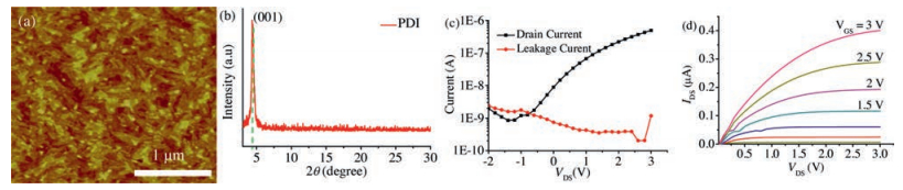
To further testify the practical performance of the silica thin film produced by spin-coating method in electronic devices application, p-type OTFTs with the silica film was constructed as shown in Fig. 1. The surface of silica was treated by O2 plasma and modified with octadecyltrichlorosilane (OTS, purchased from Aldrich Sigma) in vacuum oven at 60 ℃ for 40min [2, 7], and then 10nm p-type semiconductor dinaphtho[2, 3-b:2', 3'-f]thieno[3, 2-b] thiophene (DNTT) was deposited in vacuum thermal evaporation at a rate of 0.05Å/s under 10-4 Pa with the substrate temperature of 65 ℃. Top Au electrodes were deposited by shadow mask at a rate of 0.03Å/s under 10-4 Pa in vacuum thermal evaporation system. The AFM image (Fig. 3a) reveals that DNTT film deposited on the SiO2 film is continuous with uniform grain. The XRD patterns of DNTT film is shown in Fig. 3b, which shows characteristic peak of DNTT crystalline. This result means the silica film is suitable for growth of highly ordered and uniform DNTT. Fig. 3c and d shows the transfer curve and output curves of DNTT OTFT with silica dielectrics, from which it can be found that this device exhibits typical p-type field-effect property with well-defined linear and saturation regimes under low voltage of 4V. Low voltage operation is highly necessary for the practical application especially in wearable and portable devices. Furthermore, we got the field-effect mobility, on/off ratio and threshold voltage by calculating are 2.3 cm2 V-1 s-1, 103, and 1V respectively. The mobility is comparable to the DNTT device on the conventional thermally growth silica dielectrics (mobility ≈ 2 cm2 V-1 s-1 in ambient environment under 60V bias voltage with 300nm thermally growth SiO2), indicating the good performance of solution-processable silica dielectrics. Significantly, OTFT displays low leakage current which can be limited below 10-11 A while the OTFTs is working, which is beneficial for reduce the static power consumption.

|
Download:
|
| Fig. 3. (a) AFM image of DNTT, (b) XRD image of DNTT, (c) Transfer curve of p-type OTFT, (d) Output curves of p-type OTFT. | |
In addition to p-type OTFT, n-type device is another key component for the construction of complementary circuits that possess lower power dissipation and large noise margin compared to unipolar circuits. To further test the generality of this silica dielectrics for the n-type semiconductor, 15 nm n-type semiconductor N, N'-bis(n-octyl)-dicyanoperylene-3, 4:9, 10-bis(dicarboximide) (PDI-8CN2) was used as semiconductor layer to construct OTFT. As similar to DNTT, PDI-8CN2 also exhibits good film quality and high crystalline on silica surface, which are proved by AFM (Fig. 4a) and XRD (Fig. 4b) measurement. The transfer curve (Fig. 4c) and output curves (Fig. 4d) of PDI-8CN2 OTFT exhibit characteristic n-type field-effect property. The mobility, on/off ratio, and threshold voltage are calculated to be 0.08 cm2 V-1 s-1, 102, and —0.1 V respectively, which is comparable to the reported values (mobility ≈ 0.1 cm2 V-1 s-1 in ambient environment under 60 V bias voltage with 300 nm thermally growth SiO2) thus indicating the dielectric layer made by solution processing is suitable for both p-type and n-type OTFTs. The gate leakage is quite small as well, indicating the excellent insulating property of silica film. The OTFT measurements indicate the silica film is suitable for the construction of both p-type and n-type device with good performance.

|
Download:
|
| Fig. 4. (a) AFM image of PDI-8CN2, (b) XRD image of PDI-8CN2, (c) Transfer curve of n-type OTFT, (d) Output curves of n-type OTFT. | |
In summary, a simple solution method used to fabricate dense and smooth silica thin film under low temperature and normal atmosphere environment is successfully exploited. The thin film presents low leakage current and high electric field tolerance. When the film was used as the gate dielectric layer in OTFTs, it works well and induces high mobility and on/off ratio under low gate voltage. In addition to these good electrical performances, the simple solution method conforms to the tendency of efficient energy saving and environmental protection.
AcknowledgmentsThe authors are grateful to the National Natural Science Foundation of China (Nos. 21573277, 51503221), National Key Research and Development Program (No. 2016YFA0200700), Key Research Program of Frontier Sciences of Chinese Academy of Sciences (No. QYZDB—SSW—SLH031), Natural Sciences Foundation of Jiangsu Province (No. BK20150368), and Natural Science Foundation of Inner Mongolia of China (No. 2014JQ02).
| [1] |
C.R. Newman, C.D. Frisbie, D.A. da, S. Filho, et al., Chem. Mater. 16(2004) 4436-4451. DOI:10.1021/cm049391x |
| [2] |
X. Chen, S. Zhang, K. Wu, et al., Adv. Electron. Mater. 2(2016) 1500409. DOI:10.1002/aelm.201500409 |
| [3] |
L. Wang, J.A. Jackman, W.B. Ng, N.-J. Cho, Adv. Funct. Mater. 26(2016) 8623-8630. DOI:10.1002/adfm.v26.47 |
| [4] |
H. Zhang, N. Qiu, W. Ni, et al., Dyes Pigments 126(2016) 173-178. DOI:10.1016/j.dyepig.2015.11.024 |
| [5] |
M. Sawamoto, H. Sugino, M. Nakano, K. Takimiya, Org. Electron. 46(2017) 68-76. DOI:10.1016/j.orgel.2017.04.001 |
| [6] |
H.E. Jan, H. Hoang, T. Nakamura, et al., J. Electron. Mater. 46(2017) 3610-3614. DOI:10.1007/s11664-017-5506-9 |
| [7] |
X. Chen, Z. Xu, K. Wu, et al., Langmuir 32(2016) 9492-9500. DOI:10.1021/acs.langmuir.6b02585 |
| [8] |
A. Spende, N. Sobel, M. Lukas, et al., Nanotechnology 26(2015) 335301. DOI:10.1088/0957-4484/26/33/335301 |
| [9] |
L. Ghazaryan, E.B. Kley, A. Tunnermann, A. Szeghalmi, Nanotechnology 27(2016) 255603. DOI:10.1088/0957-4484/27/25/255603 |
| [10] |
A. Liu, Z. Guo, G. Liu, et al., Adv. Electron. Mater. 3(2017) 1600513. DOI:10.1002/aelm.201600513 |
| [11] |
L. Liu, X.M. Yu, B. Zhang, S.X. Meng, Y.Q. Feng, Chin. Chem. Lett. 28(2017) 765-770. DOI:10.1016/j.cclet.2017.03.011 |
| [12] |
T. Matsutani, T. Asanuma, C. Liu, M. Kiuchi, T. Takeuchi, Nucl. Instrum. Methods B 206(2003) 343-347. DOI:10.1016/S0168-583X(03)00759-6 |
| [13] |
D. Hegemann, U. Vohrer, C. Oehr, R. Riedel, Surf. Coat. Technol. 116- 119(1999) 1033-1036. |
| [14] |
A.H. Azman, R.M. Ayub, M.K.M. Arshad, et al., IEEE(2014), 392-395. |
| [15] |
T. Serikawa, S. Shirai, Vacuum 51(1998) 781-783. DOI:10.1016/S0042-207X(98)00290-5 |
| [16] |
W.F. Wu, B.S. Chiou, Appl. Surf. Sci. 99b(1996) 237-243. |
| [17] |
H.M. Jin, A. Felix, M. Aroyave, Chin. Chem. Lett. 18(2007) 577-580. DOI:10.1016/j.cclet.2007.02.016 |
| [18] |
C.C. Zhuang, J. Feng, H. Xu, L. Li, X.W. Liu, Chin. Chem. Lett. 27(2016) 871-874. DOI:10.1016/j.cclet.2016.01.034 |
| [19] |
S.T. Shishiyanu, O.I. Lupan, T.S. Shishiyanu, V.P. Şontea, S.K. Railean, Electrochim. Acta 49(2004) 4433-4438. DOI:10.1016/j.electacta.2004.04.034 |
| [20] |
M.M. Moslehi, S.C. Shatas, K.C. Saraswat, Appl. Phys. Lett. 47(1985) 1353-1355. DOI:10.1063/1.96278 |
| [21] |
M.M. Moslehi, K.C. Saraswat, S.C. Shatas, Appl. Phys. Lett. 47(1985) 1113-1115. DOI:10.1063/1.96347 |
| [22] |
Y.L. Chiou, C.H. Sow, G. Li, K.A. Ports, Appl. Phys. Lett. 57(1990) 881-883. DOI:10.1063/1.104265 |
| [23] |
T.T. Zhang, J.Y. Jiang, Y.H. Wang, Chin. Chem. Lett. 28(2017) 307-311. DOI:10.1016/j.cclet.2016.07.029 |
| [24] |
C. Vautrin-Ul, C. Boisse-Laporte, N. Benissad, Prog. Org. Coat. 38(2000) 9-15. DOI:10.1016/S0300-9440(99)00077-6 |
| [25] |
M.I. Alayo, I. Pereyra, M.N.P. Carreno, Thin Solid Films 332(1998) 40-45. DOI:10.1016/S0040-6090(98)01021-9 |
| [26] |
I. Frac, M. Kucinska, P. Gawrys, et al., Synth. Met. 220(2016) 194-201. DOI:10.1016/j.synthmet.2016.05.025 |
| [27] |
Z.T. Huang, C.C. Fan, G.B. Xue, et al., Chin. Chem. Lett. 27(2016) 523-526. DOI:10.1016/j.cclet.2016.01.054 |
| [28] |
L.N. Fu, B. Leng, Y.S. Li, X.K. Gao, Chin. Chem. Lett. 27(2016) 1319-1329. DOI:10.1016/j.cclet.2016.06.045 |
| [29] |
Y. Liu, L. Liu, L. Kong, L. Kang, F. Ran, Electrochim. Acta 211(2016) 469-477. DOI:10.1016/j.electacta.2016.06.058 |
| [30] |
Z. Zhang, Z. Shao, Y. Luo, et al., Polym. Int. 64(2015) 971-978. DOI:10.1002/pi.2015.64.issue-8 |
| [31] |
M. Chen, B.H. Kim, Q. Xu, B.G. Ahn, D.P. Huang, J. Membrane Sci. 360(2010) 461-468. DOI:10.1016/j.memsci.2010.05.045 |
| [32] |
R. Nisticò, D. Scalarone, G. Magnacca, Microporous Mesoporous. Mater. 248(2017) 18-29. DOI:10.1016/j.micromeso.2017.04.017 |
| [33] |
L.Y. Liu, X. Zhang, H.X. Li, et al., Chin. Chem. Lett. 28(2017) 206-212. DOI:10.1016/j.cclet.2016.07.027 |
| [34] |
D. Seyferth, G.H. Wiseman, C.P. Homme, J. Am. Ceram. Soc. 66(1983) C13-C14. |
| [35] |
M. Arai, T. Funayama, I. Nishii, et al., Japanese Patent(1987), 62-125015. |