 2017, Vol. 28


b Institute of Polymer Optoelectronic Materials and Devices, State Key Laboratory of Luminescent Materials and Devices, South China University of Technology, Guangzhou 510640, China;
c Center for Functional Nanomaterials, Brookhaven National Laboratory, Upton NY 11973, USA
Organic semiconductors are widely used in a variety of electronic devices such as organic field-effect transistors (FETs) [1-6], organic solar cells (OSCs) [7-10], and organic light-emitting diodes (OLEDs) [11-15]. For these devices, high charge mobility is typically desired and organic single-crystals are, thus, ideal materials. In principle, organic single crystals have the potential to achieve superior charge transport performance, as they have the highest degree of order in long range compared with their amorphous and polycrystalline counterparts [16-19]. In addition to the function of charge transport, other optoelectronic functions are needed to construct a working device, such as exciton generation for emission [11] and exciton dissociation for photovoltaics [7]. Only a few materials (including organic and organicinorganic hybrid materials) have good performance in multiple aspects, like charge transport, luminescence, light absorption and so on [20-25]. For example, high-mobility organic crystals typically exhibit very weak fluorescence due to the aggregationinduced quenching effect [26]. As such, multifunction is often achieved by mixing multi-components with varied functions [27-30]. Examples include chemical sensors with various composites [31-34], memory devices containing embedded nanoparticles [35, 36], photo detectors incorporated with quantum dots [37, 38], light-emitting devices based on multiple components [39-41] and solar cells with heterojunctions [8, 42, 43].
Although mixing is effective to realize multifunction, it generally reduces the crystallinity of active materials and leads to the reduction of charge mobility. Therefore, maintaining the ordered molecular packing within the multi-component active materials is needed. Efforts have been made to the fabrication of multifunctional composites based on single crystals. For example, functional nanoparticles and nanorods have been incorporated into well-ordered inorganic single crystals, organic single crystals and metal-organic framework single crystals to get materials with multiple functions [44-48]. However, design of single crystal composites where foreign materials are distributed inside single crystals to achieve multiple functions has not been appreciated in the field of organic electronics. In this article, we demonstrate that fluorescent PBI nanofibers, the guest, can be incorporated into the solution-grown aligned 6, 13-bis(triisopropylsilylethynyl)-pentacene (TIPS-pentacene) single crystals, the host, by a two-step method to form single-crystal composites (Fig. 1A). These singlecrystal composites exhibit additional luminescence performance while maintaining high charge carrier mobility.

|
Download:
|
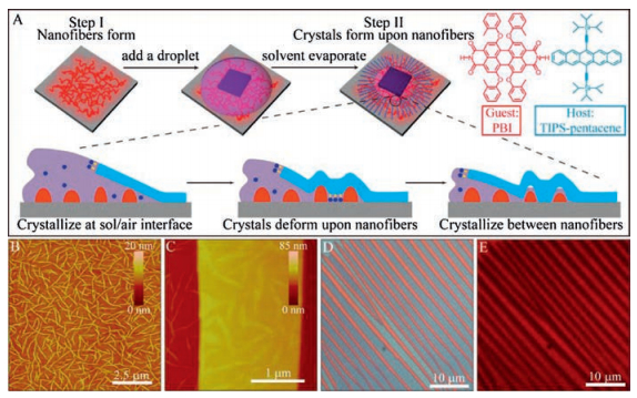
| Fig. 1. Schematic representations of the two-step preparation method for single-crystal composites together with the morphologies of the products in each step. (A) Schematic representations of the method: TIPS-pentacene crystallizes from a receding droplet on a substrate containing preformed PBI nanofibers. Crystals first grow at the interface of solution and air. As the solvent separating the crystals and the nanofibers evaporates, crystals contact the nanofibers and deform. Further crystallization fills the space between the nanofibers. (B) An AFM image of spin-coated PBI nanofibers. (C) An AFM image of single-crystal composites, showing fibrous humps on the top surface. (D, E) Optical and fluorescence microscopy images showing the light blue crystal ribbons in (D) emit red fluorescence in (E). | |
TIPS-pentacene [49] was selected as the host and a recently reported PBI gelator [50] as the guest (Fig. 1A). TIPS-pentacene crystallizes easily and has the potential to exhibit high mobility [51] while TIPS-pentacene films have very weak fluorescent emission [52]. On the other hand, the PBI molecules self-assemble through hydrogen bonding into highly fluorescent nanofibers [50]. The nanofiber guest and the crystal host were interfaced together using a two-step method as described in Fig. 1. First, PBI nanofibers formed after PBI solutions (0.1mg/mL) were spin-coated on a substrate, as imaged by AFM (Fig. 1B). The nanofibers are 2–10nm in height and 0.4–1.9 μm in length. Second, the TIPS-pentacene crystallizes in the presence of the PBI nanofibers. A droplet of TIPS-pentacene solution with an orthogonal solvent (hexane, 0.3mg/mL) was added on thePBI fibers. As the solventevaporated, crystals formed through a DPC process in which directional receding of a droplet leads to crystal alignment [53, 54]. Interestingly, the obtained TIPS-pentacene crystals (Fig. 1D) exhibit well-aligned ribbon shapes similar to those of crystals grown in the absence of the PBI nanofibers [55, 56] (Fig. S1 in Supporting information). The well-aligned long crystals have a width of 2.3–6.9 μm and a height of 27–57nm, as measured from AFM images. As the crystals do not cover the substrate surface completely, the exposed PBI nanofibers between the crystals were easily washed away and those covered by the crystals can be imaged by fluorescence microscopy. In OM and fluorescence microscopy, red fluorescence emission was observed exactly at the locations of the crystals, indicating the coexistence of the fluorescent PBI and the TIPS-pentacene crystals (Figs. 1D and E).

|
Download:
|
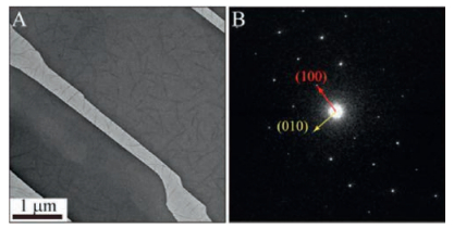
| Fig. 2. (A) TEM image showing the coexistence of nanofibers and single crystals (dark ribbons). (B) SAED pattern showing the single crystallinity. | |
Similarly, the coexistence of both components was directly imaged by TEM (Fig. 2A). Furthermore, how the PBI nanofibers distributed together with the TIPS-pentacene crystals was examined by imaging both the top and bottom surfaces of the crystals. The AFM images show fibrous humps on the top surface (Fig. 1C) and fibrous pits on the bottom surface (Fig. 3A), instead of the typical smooth terraces [55]. The sizes and morphologies of these humps and pits are similar to those of the PBI nanofibers, indicating that the nanofibers penetrate into the crystals. Despite the presence of the nanofibers in the crystals, the host crystals still maintain their single-crystalline nature. Selected-area electron diffraction (SAED) of a large area (diameter of 6.5 μm, Fig. 2B), including fibers, gives a single set of diffraction spots consistent with those of TIPS-pentacene single crystals [57]. And the singlecrystallinity was reconfirmed by polarized OM (Fig. S2 in Supporting Information). Therefore, the OM, TEM, AFM and SAED evidences demonstrate that we obtained the single-crystal composites with PBI nanofiber guest incorporated in the TIPS-pentacene crystal host.

|
Download:
|
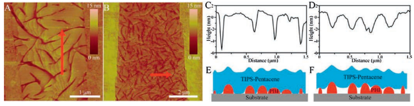
| Fig. 3. AFM images of bottom surfaces along with scheme representations for two single-crystal composites prepared with different TIPS-pentacene concentrations of 0.3 mg/mL (A, C, E) and 0.05 mg/mL (B, D, F). (A, B) AFM images of bottom surfaces. (C, D) Cross section curves showing the pit depth (direction follows red arrows). (E, F) Schematic representations showing how deep the nanofibers penetrating into the crystals. | |
Next, the mechanism of the single-crystal composites form is investigated. On one hand, the fibrous humps (Fig. 1C) observed on the top surface of the crystals indicate that the smooth crystalline terraces are deformed by the PBI fibers into rough surfaces when the crystals contact the nanofibers. On the other hand, the deep pits (Fig. 3A) on bottom surface of the crystals suggest that the crystals continue to grow to fill in the gaps between the nanofibers after they contact each other. Based on these observations, we propose a mechanism by which the crystals incorporate the nanofibers through the following 3 steps (Fig. 1A). 1) The TIPS-pentacene crystallizes mainly at the interface of solution and air into ribbons, while the PBI nanofibers locate on another interface of solution and substrate. The solvent between the ribbons and the nanofibers separates them from each other and prevents mutual disturbance. 2) As the solvent in between gradually evaporates, the crystal ribbons start to contact the nanofibers and slightly deform due to the flexibility of organic crystals [58, 59]. 3) Subsequently, the crystal ribbons continue to grow into the space between the nanofibers. As a result, the nanofibers are finally incorporated inside the crystals. One supporting evidence for this mechanism is the AFM imaging of the crystals grown from solutions of a lower concentration (Fig. 3B). The bottom surface exhibits fibrous pits that are much shallower than those on the crystals grown from solution of a higher concentration (Figs. 3C and D). The depth of the pits suggests how deep the nanofibers penetrate into the crystals (Figs. 3E and F). The shallow pits indicate that crystallization in step 3 fills in partially the space between the nanofibers, as shown in Fig. 3F.
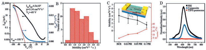
After obtaining the single-crystal composites, we proceed to examine their electronic properties. FETs were fabricated with Au as the source and drain electrodes (Fig. 4C, inset) and tested in the saturation regime under N2 atmosphere. For comparison, we studied the composites containing increasing nanofiber densities (Fig. S3 in Supporting Information) that were realized by using PBI solutions of varying concentrations (0–0.1 mg/mL), with the FET parameters summarized in Fig. 4C, Fig. S4 and Table S1 in Supporting information. The hole mobility of the composites decreases with increasing nanofiber densities, while the on-to-off current ratios (Ion/Ioff > 105) and threshold voltages (VT) are similar. Without nanofibers, the substrates have a root mean square roughness (Rq) of 0.4 nm and the TIPS-pentacene single crystals exhibit an average hole mobility of 4.10 ± 1.79 cm2 V-1 s-1 that is close to the previous report [56]. Using a PBI solution of 0.02–0.1 mg/mL for spin coating, nanofibers are clearly seen in the AFM images (Fig. S3 in Supporting Information), with the increasing substrate roughness (Rq: 0.5–2.1 nm) and the nanofiber surface coverage (θnanofiber: 10.6%–26.4%). Accordingly, the mobility drops from 3.29 ± 1.30 to 1.57 ± 0.72 cm2 V-1 s-1. At the highest concentration of the PBI solution we used (0.1 mg/mL), the nanofiber surface coverage reaches 26.4% while the single-crystal composites still exhibit mobility more than 1 cm2 V-1 s-1 (maximum: 3.34 cm2 V-1 s-1, Figs. 4A–B). At an even higher PBI concentration (e.g., 0.2 mg/mL), crystals fail to grow into well-aligned ribbons possibly because the dense fiber networks greatly affect the stable receding of the droplet for crystallization.

|
Download:
|
| Fig. 4. FET characteristics and fluorescence emission spectra of various single-crystal composites. (A) Typical transfer characteristic of the FETs (0.1 mg/mL PBI and 0.3 mg/mL TIPS-pentacene) under p-channel operation mode. (B) Histogram of the hole mobility of 50 FETs. (C) Hole mobility of single-crystal composites prepared using PBI solutions of increasing concentrations (0–0.1 mg/mL). The surface coverage of the PBI nanofibers (θnanofiber) measured before crystallization is also plotted. Inset: A schematic representation of the FET configuration, where S is the source, D the drain, G the gate, L the channel length and W the channel width. L was measured from the real channel length and W was measured from the contacting area of the crystals that cross the S and D electrodes. W was calculated by the equation: W = Σ(W1 + W2)/2. (D) Fluorescence emission spectra of single-crystal composites, PBI nanofibers and TIPS-pentacene single crystals (λexc = 532 nm). | |
The relatively high mobility suggests that the crystallization in the empty space between the nanofibers (Fig. 1A) results in contact between the crystals and the dielectric substrate to form the conductive channel. As a lower concentration (0.05 mg/mL) of TIPS-pentacene was used for crystallization, the empty space was only partial filled with the crystals (Fig. 3B), leading to poor contact between the crystal and the dielectric and much lower mobility of 0.45 ± 0.19 cm2 V-1 s-1 (Figs. S5D–F in Supporting information). The introduction of nanofibers brings defects to the conductive channels and causes the decease of mobility. In FETs, the conductive channel of the charge carriers forms at the semiconductor/dielectric interface [60]. The nanofibers on the dielectric surface prevent the crystals to cover the dielectric completely. Consequently, the dielectric is interfaced with both the nanofiber and the crystal. The existence of the nanofibers impedes slightly the motion of holes in the channel. Previous work has shown that roughening dielectric surface results in dramatically reduced mobility of polycrystalline or amorphous organic semiconductors, especially as Rq is over 2 nm [61-63]. Interestingly, the mobility in this work does not greatly decrease even though about 26.4% of the channel area is occupied by the nanofibers, indicating the advantage of single-crystallinity and suggesting the possibility to endow the semiconducting crystal hosts with extrinsic properties from guest materials. In this case, the PBI nanofibers contribute their fluorescent property, as shown by the photoluminescence spectra (Fig. 4D). Clearly, the TIPS-pentacene single crystals have a very weak fluorescence emission while the singlecrystal composites emit a red emission with a peak similar to that of the PBI nanofibers, in consistent with the fluorescence microscopy image (Fig. 1E). The slight difference of 6 nm in the emission peaks suggests the electronic interaction between the PBI nanofibers and the TIPS-pentacene single crystals. The fluorescence property and the high charge mobility indicate that the obtained single-crystal composites might be promising for constructing organic light emitting devices.
In summary, we have demonstrated a solution method to prepare composites consisting of high-mobility TIPS-pentacene single-crystals and fluorescent PBI nanofibers. From a droplet receding on a substrate, the crystals form at the solution-air interface and, then, contact the nanofibers that settle at another interface between the substrate and the solution. Further crystallization allows incorporation of the nanofiber guest into the crystal host, leading to the composite structure. Essentially, the crystallization and incorporation events are separated spatially and proceed in a sequential fashion. Consequently, the singlecrystalline molecular packing of TIPS-pentacene is maintained in the composites that exhibit hole mobility above 1 cm2 V-1 s-1. And the nanofiber guest contributes the fluorescence property that the crystal host lacks. It is widely recognized that the integration of superior charge transport and fluorescence properties is challenging and highly desired for organic electronics and this goal has been recently achieved by rational molecular design and fine tuning of molecular packing [20]. Instead of adopting a single molecule, this work demonstrates an alternative approach to combine two components. By demonstrating composites with mixed functional components as well as long-range ordering in molecular packing, this work provides a strategy to achieve highperformance and multifunctional organic electronic devices based on single crystals through rational selection of host-guest pairs.
AcknowledgmentsThis work was supported by the 973 Program (No. 2014CB643503), National Natural Science Foundation of China (Nos. 51625304, 51373150, 51461165301, 51573055) and the Open Foundation Project of the State Key Lab of Silicon Materials (No. SKL2017-08). This research used resources of the Center for Functional Nanomaterials, which is a U.S. DOE Office of Science Facility, at Brookhaven National Laboratory under Contract No. DESC0012704.
Appendix A. Supplementary dataSupplementary data associated with this article can be found, in the online version, at http://dx.doi.org/10.1016/j.cclet.2017.08.011.
| [1] |
C.L. Wang, H.L. Dong, W.P. Hu, Y.Q. Liu, D.B. Zhu, Chem. Rev. 112(2012) 2208-2267. DOI:10.1021/cr100380z |
| [2] |
H. Sirringhaus, Adv. Mater. 26(2014) 1319-1335. DOI:10.1002/adma.201304346 |
| [3] |
H.L. Dong, X.L. Fu, J. Liu, Z.R. Wang, W.P. Hu, Adv. Mater. 25(2013) 6158-6182. DOI:10.1002/adma.201302514 |
| [4] |
J.G. Mei, Y. Diao, A.L. Appleton, L. Fang, Z.N. Bao, J. Am. Chem. Soc. 135(2013) 6724-6746. DOI:10.1021/ja400881n |
| [5] |
A. Liess, M. Stolte, T. He, F. Würthner, Mater. Horiz. 3(2016) 72-77. DOI:10.1039/C5MH00167F |
| [6] |
Y.G. Zhen, H.L. Dong, L. Jiang, W.P. Hu, Chin. Chem. Lett. 27(2016) 1330-1338. DOI:10.1016/j.cclet.2016.06.023 |
| [7] |
C.W. Tang, Appl. Phys. Lett. 48(1986) 183-185. DOI:10.1063/1.96937 |
| [8] |
S. Günes, H. Neugebauer, N.S. Sariciftci, Chem. Rev. 107(2007) 1324-1338. DOI:10.1021/cr050149z |
| [9] |
A. Mishra, P. Bäuerle, Angew. Chem. Int. Ed. 51(2012) 2020-2067. DOI:10.1002/anie.201102326 |
| [10] |
Y.Z. Lin, X.W. Zhan, Mater. Horiz. 1(2014) 470-488. DOI:10.1039/C4MH00042K |
| [11] |
C.W. Tang, S.A. Vanslyke, Appl. Phys. Lett. 51(1987) 913-915. DOI:10.1063/1.98799 |
| [12] |
A.C. Grimsdale, K.L. Chan, R.E. Martin, P.G. Jokisz, A.B. Holmes, Chem. Rev. 109(2009) 897-1091. DOI:10.1021/cr000013v |
| [13] |
X.K. Liu, Z. Chen, C.J. Zheng, et al., Adv. Mater. 27(2015) 2378-2383. DOI:10.1002/adma.v27.14 |
| [14] |
S.Y. Lee, T. Yasuda, Y.S. Yang, Q.S. Zhang, C. Adachi, Angew. Chem. Int. Ed. 53(2014) 6402-6406. DOI:10.1002/anie.201402992 |
| [15] |
D.D. Zhang, M.H. Cai, Y.G. Zhang, D.Q. Zhang, L. Duan, Mater. Horiz. 3(2016) 145-151. DOI:10.1039/C5MH00258C |
| [16] |
V. Podzorov, MRS Bull. 38(2013) 15-27. DOI:10.1557/mrs.2012.306 |
| [17] |
H.Y. Li, G. Giri, J.B.H. Tok, Z.N. Bao, MRS Bull. 38(2013) 34-42. DOI:10.1557/mrs.2012.309 |
| [18] |
C. Reese, Z.N. Bao, Mater. Today 10(2007) 20-27. |
| [19] |
X.K. Gao, Y.B. Hu, J. Mater. Chem. C 2(2014) 3099-3117. DOI:10.1039/C3TC32046D |
| [20] |
J. Liu, H.T. Zhang, H.L. Dong, et al., Nat. Commun. 6(2015). |
| [21] |
W.Y. Nie, H.H. Tsai, R. Asadpour, et al., Science 347(2015) 522-525. DOI:10.1126/science.aaa0472 |
| [22] |
W.G. Zhu, R.H. Zheng, Y.G. Zhen, et al., J. Am. Chem. Soc. 137(2015) 11038-11046. DOI:10.1021/jacs.5b05586 |
| [23] |
J. Liu, J.Y. Liu, Z.C. Zhang, et al., J. Mater. Chem. C 5(2017) 2519-2523. |
| [24] |
J. Li, J. Liu, Y.G. Zhen, et al., J. Mater. Chem. C 3(2015) 10695-10698. DOI:10.1039/C5TC02254A |
| [25] |
M.Y. Chen, Y. Zhao, L.J. Yan, et al., Angew. Chem. Int. Ed. 56(2017) 722-727. DOI:10.1002/anie.201608131 |
| [26] |
J. B. Birks, Photophysics of Aromatic Molecules, Wiley, London, 1970.
|
| [27] |
A. Opitz, M. Bronner, W. Brütting, J. Appl. Phys. 101(2007). |
| [28] |
C. Li, L. Duan, H.Y. Li, Y. Qiu, Org. Electron. 14(2013) 3312-3317. DOI:10.1016/j.orgel.2013.09.039 |
| [29] |
L.N. Fu, B. Leng, Y.S. Li, X.K. Gao, Chin. Chem. Lett. 27(2016) 1319-1329. DOI:10.1016/j.cclet.2016.06.045 |
| [30] |
W.H. Zhang, B.J. Jiang, P. Yang, Chin. Chem. Lett. 27(2016) 1339-1344. DOI:10.1016/j.cclet.2016.06.044 |
| [31] |
B. Kang, M. Jang, Y. Chung, et al., Nat. Commun. 5(2014). |
| [32] |
S.L. Ji, H.B. Wang, T. Wang, D.H. Yan, Adv. Mater. 25(2013) 1755-1760. DOI:10.1002/adma.v25.12 |
| [33] |
J. Huang, J. Miragliotta, A. Becknell, H.E. Katz, J. Am. Chem. Soc. 129(2007) 9366-9376. DOI:10.1021/ja068964z |
| [34] |
L. Torsi, G.M. Farinola, F. Marinelli, et al., Nat. Mater. 7(2008) 412-417. DOI:10.1038/nmat2167 |
| [35] |
C.W. Tseng, Y.T. Tao, J. Am. Chem. Soc. 131(2009) 12441-12450. DOI:10.1021/ja904882m |
| [36] |
S.M. Wang, C.W. Leung, P.K.L. Chan, Org. Electron. 11(2010) 990-995. DOI:10.1016/j.orgel.2010.03.020 |
| [37] |
S.A. McDonald, G. Konstantatos, S.G. Zhang, et al., Nat. Mater. 4(2005) 138-142. DOI:10.1038/nmat1299 |
| [38] |
T. Rauch, M. Böberl, S.F. Tedde, et al., Nat. Photonics 3(2009) 332-336. DOI:10.1038/nphoton.2009.72 |
| [39] |
F. Dinelli, R. Capelli, M.A. Loi, et al., Adv. Mater. 18(2006) 1416-1420. DOI:10.1002/(ISSN)1521-4095 |
| [40] |
C. Rost, S. Karg, W. Riess, et al., Appl. Phys. Lett. 85(2004) 1613-1615. DOI:10.1063/1.1785290 |
| [41] |
S. Hotta, T. Yamao, S.Z. Bisri, T. Takenobu, Y. Iwasa, J. Mater. Chem. C 2(2014) 965-980. DOI:10.1039/C3TC31998A |
| [42] |
B.C. Thompson, J.M.J. Fréchet, Angew. Chem. Int. Ed. 47(2008) 58-77. DOI:10.1002/(ISSN)1521-3773 |
| [43] |
P. Cheng, X.W. Zhan, Mater. Horiz. 2(2015) 462-485. DOI:10.1039/C5MH00090D |
| [44] |
Y.J. Liu, W.T. Yuan, Y. Shi, et al., Angew. Chem. Int. Ed. 53(2014) 4127-4131. DOI:10.1002/anie.201310712 |
| [45] |
G. Lu, S.Z. Li, Z. Guo, et al., Nat. Chem. 4(2012) 310-316. DOI:10.1038/nchem.1272 |
| [46] |
Y.J. Liu, H.D. Zang, L. Wang, et al., Chem. Mat. 28(2016) 7537-7543. DOI:10.1021/acs.chemmater.6b03589 |
| [47] |
M. Sindoro, Y.H. Feng, S.X. Xing, et al., Angew. Chem. Int. Ed. 50(2011) 9898-9902. DOI:10.1002/anie.v50.42 |
| [48] |
Y.L. Yan, C. Zhang, J.N. Yao, Y.S. Zhao, Adv. Mater. 25(2013) 3627-3638. DOI:10.1002/adma.v25.27 |
| [49] |
J.E. Anthony, J.S. Brooks, D.L. Eaton, S.R. Parkin, J. Am. Chem. Soc. 123(2001) 9482-9483. DOI:10.1021/ja0162459 |
| [50] |
Z.Q. Xie, V. Stepanenko, B. Fimmel, F. Würthner, Mater. Horiz. 1(2014) 355-359. DOI:10.1039/c3mh00159h |
| [51] |
Y. Diao, B.C.K. Tee, G. Giri, et al., Nat. Mater. 12(2013) 665-671. DOI:10.1038/nmat3650 |
| [52] |
A.D. Platt, J. Day, S. Subramanian, J.E. Anthony, O. Ostroverkhova, J. Phys. Chem. C 113(2009) 14006-14014. |
| [53] |
H.Y. Li, B.C.K. Tee, J.J. Cha, et al., J. Am. Chem. Soc. 134(2012) 2760-2765. DOI:10.1021/ja210430b |
| [54] |
H.Y. Li, C.C. Fan, M. Vosgueritchian, B.C.K. Tee, H.Z. Chen, J. Mater. Chem. C 2(2014) 3617-3624. DOI:10.1039/c3tc32431a |
| [55] |
H.Y. Li, B.C.K. Tee, G. Giri, et al., Adv. Mater. 24(2012) 2588-2591. DOI:10.1002/adma.v24.19 |
| [56] |
S. Liu, J.K. Wu, C.C. Fan, et al., Sci. Bull. 60(2015) 1122-1127. DOI:10.1007/s11434-015-0817-9 |
| [57] |
G. Xue, C. Fan, J. Wu, et al., Mater. Horiz. 2(2015) 344-349. DOI:10.1039/C4MH00211C |
| [58] |
A.L. Briseno, R.J. Tseng, M.M. Ling, et al., Adv. Mater. 18(2006) 2320-2324. DOI:10.1002/(ISSN)1521-4095 |
| [59] |
M.A. Reyes-Martinez, A.J. Crosby, A.L. Briseno, Nat. Commun. 6(2015). |
| [60] |
J. Zaumseil, H. Sirringhaus, Chem. Rev. 107(2007) 1296-1323. DOI:10.1021/cr0501543 |
| [61] |
S.E. Fritz, T.W. Kelley, C.D. Frisbie, J. Phys. Chem. B 109(2005) 10574-10577. DOI:10.1021/jp044318f |
| [62] |
L.L. Chua, P.K.H. Ho, H. Sirringhaus, R.H. Friend, Adv. Mater. 16(2004) 1609-1615. DOI:10.1002/(ISSN)1521-4095 |
| [63] |
S. Steudel, S. De Vusser, S. De Jonge, et al., Appl. Phys. Lett. 85(2004) 4400-4402. DOI:10.1063/1.1815042 |