 2017, Vol. 28


Molecular electronics describes a field that seeks to understand charge-transport properties of single molecules and their ensembles. Ultimately this may pave the way for electronic components made of molecular building blocks. This visionary concept was first sketched out in 1974 by Arieh Aviram and Mark Ratner [1]. In their theoretical paper, they suggested that a single molecule could function as a rectifier. If it comes true, computational architectures may be built molecule-by-molecule, namely, in a "bottom-up" way. In the past 40 years (especially in the last 20 years), benefiting from the rapid development of technology, molecular electronics has generated more and more excitement supported by constantly growing theoretical and experimental achievements. On one hand, the prospect of molecular-scale electronics offers a potential alternative/addition to complementary metal-oxide-semiconductor (CMOS) technology that relies on "top-down" methods and is expected to face fundamental limitations on further scaling (e.g., direct source-drain electron tunneling) in the next decade or so [2]. On the other hand, synthetic method promises a molecular-level control of properties. Well-designed organic molecules represent a class of inexpensive, flexible and easy-processing materials compared with their inorganic counterparts. These advantages of organic materials have been well exploited in "bulk" thin-film devices, such as light-emitting diodes (OLEDs) [3], organic fieldeffect transistors (OFETs) [4] and organic photovoltaics (OPVs) [5], some of which have already been successfully commercialized. On this basis, in spite of even more challenges, many efforts have been concentrated on pushing organic electronics into the nano/atomic realms. To date, individual molecules equipped with unique optoelectronic properties have successfully shown their potential for molecular scale electronics [6].
However, silicon-based technology is unlikely to be replaced anytime soon and there remain enormous challenges along the way to molecular electronics. Before we can actually set out to build computers out of molecules, understanding charge transport of single molecules or a small collection of molecules is of fundamental importance. This requires making reliable contacts to molecular components, which means a degree of control with atomic accuracy. In the early 1970s, Bernhard Mann and Hans Kuhn successfully measured the tunneling current through a monolayer of molecules [7]. Then development of scanning probe microscopy (SPM) since 1980s enabled some of the earliest attempts to image and measure individual molecules on surfaces. By using a scanning tunneling microscopy (STM) or conducting probe atomic force microscopy (cpAFM) tip, single molecules can be repeatedly addressed and in this way fundamental insights into how electron transport occurs within molecules and their contacts can be provided. SPM techniques are still among the most important testbeds today and continuously making contributions to our understanding of the principles in the field of molecular electronics. For instance, STM break junction (STM-BJ) technique provides a reliable tool to investigate the charge transport properties on a single-molecule level. By repeating the BJ cycles for hundred to thousand times, STM-BJ could give a large database for subsequent statistical analysis [8]. Moreover, an electrochemical gating can be conveniently added to manipulate the energy alignment and molecular redox processes for a single-molecule junction [9]. In the last few years, Zhang and coworkers systematically studied the electron-transport characteristics of a series of oligo(phenyleneethynylene) (OPE) molecular wires with STM-BJ method. The results showed that the electron-transport pathways of "core-shell"-structured OPE molecules are strongly affected by the size of the side group [10], and the conductance of OPE molecular junctions are strongly affected by the coupling strength between the two phenyl-ethynyl-phenyl p systems [11]. These studies provide useful guidelines for further research in single-molecule electronics.
Besides STM-BJ, mechanically controllable break junction (MCBJ) technique is another efficient testbed for single-molecule junctions. MCBJ was first used to measure the conductance of single molecules by Reed et al. in 1997 [12]. Though MCBJ is lack of imaging function compared to STM-BJ, it has been widely used in the measurements of single-molecule electronics for its unique advantages, such as precisely controlled gap distance, high mechanical stability, and good compatibility with other systems [13].Very recently, Hong et al. developed an approach to detect the dihydroazulene photo-thermal reaction by using single-molecule MCBJtechnique[14].Inthisstudy, the product ratios observed in the junctions does not follow those observed in solution studies, which revealed that molecular junctions have the possibility to tailor product ratios in chemical reactions.
On the other hand, from an application perspective, integrated circuits of metal-molecule-metal junctions require robust electrode geometries that can be prepared over large areas. Given the feature size of a molecule (typically a few nanometers), making contact electrodes with a nanometer gap (dimension varies depending on the actual size of a target molecule) is the first crucial step for the realization of practical molecular electronic devices. To this end, a variety of platforms have been experimentally developed to wire molecules into circuits with atomically defined precision, which, are generally referredto as "nanogapelectrodes"[15]. Based onnanogap electrodes, various molecular electronic devices such as molecular rectifiers [16, 17], switches [18-23], transistors [24, 25] have been successfully fabricated. More recently, fundamental new concepts beyondsimple descriptionsof electronic transport, suchas quantum interference, thermoelectronics, mechanics and spintronics have also been reported [26].
Compared with the junctions built on a very limited number of molecules, self-assembled monolayers (SAMs) represent a more reproducible molecular system for the fabrication of electronic devices, and are more amenable to mass production and integration. However, direct vapor deposition of metals onto SAMs has proven to be very invasive and damaging. Filamentary paths of metals or damages to the molecules normally result in a high percentage of short-circuits. To address this problem, several soft contacting methods [27] have been accordingly developed, and functional molecular electronic applications have been demonstrated.
This review focuses on recent advances and efforts regarding the main challenges of device fabrication andfunctionality in the field of molecular-scale electronics.Fabrication of nanogap electrodes for single-molecule junctions, and self-assembled-monolayers (SAMs) of functional molecules for solid-state devices are highlighted. The prospect of molecular-scale electronics is also discussed.
2. The fabrication and application of nanogap electrodesNanogap electrodes, a pair of electrodes with a nanometer separation, are regarded as fundamental tools for the fabrication of molecular devices and circuits. To preparenanogap electrodes with suitable separations for target molecules, various methods have been developed, including mechanical controllable break junctions (MCBJ) [12, 13, 28], electrochemical and chemical deposition [29], electromigration [30], electron-beam lithography (EBL) [31], focused ion beam lithography (FIB) [32], and other techniques. Based on these methods, nanogap electrodes are prepared and applied. However, most of the existing methods have complicated processes and high-cost, which limits their application in mass production. Developing new fabrication methods of nanogap electrodes is still a challenge in the field of molecular-scale electronics. Here we will introduce several examples of fabricating nanogap electrodes and their applications.
2.1. Electrochemical cellsMicroelectrodes with excellent electrochemical characteristics are very powerful tools for the exploration of electrochemical properties in ultrasmall volumes [33].Capable of providing highly confined systems with ultrahigh sensitivity, nanogap electrodes are a potential candidate for single molecule analysisby using electrochemical method.
Innovatively, we introduced nanogap electrodes into electrochemistry systems, and prepared electrochemical microcells with volumes ranging from femtoliter to attoliter based on micro-and nanogap electrodes (Fig. 1a) [34]. In this study, we found that space confinement effect in attoliter cells would gradually dominate and change the diffusion mode of electrochemical active molecules, from mostly spherical to planar diffusion. The reversible cycle of molecules between the close-by working and reference/counter microelectrodes contributed to a positive feedback effect, which would be suitable for trace or even single-molecule electroanalysis.

|
Download:
|
| Fig. 1. (a) Schematic view of electrochemical cells prepared by photolithography on Si/SiO2 wafer chips. Adapted with permission [34]. Copyright 2010, American Chemical Society. (b) Schematic diagram of the fabricated photoswitch device. Adapted with permission [37]. Copyright 2010, Wiley-VCH. (c) Schematic diagram of graphene nanogap electrodes and CuPc devices based on graphene nanogap electrodes. Adapted with permission [41]. Copyright 2010, AIP Publishing LLC. (d) The fabrication of nanogap structures by nanosphere lithography (left), SEM images of arrays based on different numbers of located nanospheres and nanogap electrodes with six junctions (right). Adapted with permission [44]. Copyright 2017, Wiley-VCH. | |
To further realize the selective detection of trace organic functional molecules, we fabricated single micropore electrodes in situ on silicon chips by focused ion beam (FIB) lithography [35]. For the good electron donating properties of n-type semiconductors, we investigated the different electrochemical behaviors of electron donor (TTF, tetrathiafulvalene) and acceptor (TCNQ, tetracyanoquinodimethane)on the surface of microelectrodes and realized the selective detection of organic functional molecules.
2.2. Organic optoelectronics based on nanogap electrodesAs is well known, the blend of poly(3-hexylthiophene): [6, 6]-phenyl-C61-butyric acid methyl ester (P3HT: PCBM) is a typical systemthat has been extensively studied in organic solar cells [36].To explore the effect of electrode distance on device efficiency, we fabricated high-performance organic photoswitches of P3HT:PCBM based on gold nanogap electrodes (Fig. 1b) [37]. Due to the superior photoelectric properties of P3HT: PCBM and the efficient charge collection at the nanogap electrodes, these devices showed an optimum performance with gap width around 75-100 nm, and had the highest on/off ratio of 10000 at 1 mV bias. Moreover, after repeated measurements or kept in air for nearly two months, the optoelectronic devices had no obvious degradation. The excellent performances, such as low energy consumption, low cost and high stability in ambient atmosphere, exhibited the great prospect of P3HT: PCBM blends and nanogap electrodes in molecular-scale electronics.
Graphene with excellent electronic and mechanical properties is an ideal material as electrodes [38]. However, few methods have been developed to fabricate graphene nanogap electrodes. Prinsetal. reported the feedback-controlled electroburning to prepare graphene nanogap electrodes [39]. Though the separations of prepared gaps were as small as 1-2 nm, the electrode geometry and the gap size could not be well controlled. Cao et al. developed the dash-line lithography (DLL) tocreate molecular-scale graphene gaps [40]. DLL method largely simplified the process of preparation and improved the yield of stable molecular devices.
We reported the methods of preparing graphene and graphene oxide (GO) nanogap electrodes by atomic force microscopy (AFM) nanolithography (Fig. 1c) [41]. Superior toelectroburning, the separations of these prepared graphene nanogap electrodes could be easily controlled by the diameter of AFM tips and the applied force. Withthismethod, the smallest gap could be down to 10 nm.Basedon the prepared graphene electrodes, we prepared bottom-contactthin filmdevicesofcopper phthalocyanine (CuPc)(Fig. 1c).Becauseof the well-matched energy level between CuPc and graphene material, the devices exhibited high performances, such as high stability, high on/ off ratio (up to 800). These results indicated that graphene nanogap electrodes have good prospects in molecular-scale electronics.
2.3. Nanosphere lithographyNanosphere lithography (colloidal lithography, or naturallithography, NSL) is a very useful method for preparing nanomaterials and nanostructures, which was first reported by Fischer and Zingsheim in 1981 [42, 43]. Recently, by using nanosphere lithography, we successfully fabricated sub-10 nm nanogap electrodes/arraysand applied them to the DNA-based molecular junctions to conduct electrical measurements (Fig. 1d) [44]. Polystyrene nanospheres could form a closely packed monolayer structure by self-assembly and act as a mask to construct nanogaps. By controlling the plasmatreatment time, nanogaps with different lengths, such as 50 nm, 20 nm, sub-10 nm (50% yield), even sub-5 nm (5% yield) could be easily prepared.The current-voltage measurements of DNA junction were also conducted, and the results were consistent with previous works. Nanosphere lithography is an effective and promising method to fabricate nanogap electrodes with low cost and simple process.
3. The soft top-contacts of SAM-based molecular junctionsSelf-assembled monolayer is an ordered monolayer of molecules absorbing on the surface of substrates through chemical bonds without human intervention [45].Compared with single molecule or a few molecules in molecular junctions, SAMs have good stabilities and reproducibilities, showing a great potential for application in molecular junctions.
Generally, top contact electrodes of SAMs-based vertical junctions are fabricated by direct evaporation of metals, which may damage the SAM and cause short circuits [27, 46]. To solve these problems, several non-destructive methods have been developed. Loo et al. first introduced transfer printing to fabricate soft topcontact electrodes in Au/1, 8-octanedith-iol/GaAs junctions [47]. By contacting the elastomeric poly(dimethylsiloxane) (PDMS) stamp coated Au film with SAM-modified GaAs, they successfully printed the Au film onto SAMs and realized the soft top-contacts. Vilan et al. developed the method lift-off float-on (LOFO) and transferred the metal film onto SAMs via capillary interactions [48]. However, the wrinkling of Au films and additional air gaps between molecule layer and metal film limited LOFO's further application. Improving the LOFO method by transferring top metal layer with a hydrophobic polymer, Shimizu et al. developed the method polymer-assisted lift-off (PALO) and solved the wrinkling problem in LOFO [49]. Moreover, using liquid metals, such as Hg [50] and eutectic galliumindium (EGaIn) [51], is also an efficient method to form nondestructive top-contacts. There are mainly two ways for liquid metals to form soft contacts: (1) Molecules are first absorbed on the liquid metal, then the modified metal drop is brought into contact with the second electrode.(2)Molecules are absorbed on the second electrode first, then the liquid metal contacts with them. The liquid metal contact is relatively stable and can effectively prevent problems such as mechanical damage and metal atom penetration. Besides the direct contacts between metal electrode and SAM, inserting a buffer interlayer between them is also aneffective way to realize soft top-contacts. Mbindyo et al. reported Ag nanoparticles as a buffer layer in the fabrication of in-wire monolayer junctions [52]. Akkerman et al. reported the conductor polymer poly(4-styrenesulphonic acid) (PEDOT: PSS) as a interlayer in molecular junctions in large-area with diameters up to 100 μm [53]. These junctions were very stable and had a shelf life of more than several months. However, there are also some problems in this method, such as the low processing temperature (below 50 ℃) and the unclear structures of interface.
Graphene has atomic thickness, high conductivity and high transparency, making it a potential candidate acting as an interlayer for soft top-contacts. Furthermore, for the high flexibility of graphene, it can form a close contact with SAMs. Wang et al. reported multilayer graphene films prepared by chemical vapor deposition (CVD) as a top transparent electrode in molecular electronic junctions. This work showed that graphene could be a good alternative to PEDOT: PSS as a interlayer between SAMs and top electrodes [54].
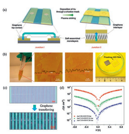
Compared with CVD graphene films, reduced graphene oxide (rGO) films have many advantages: (1) rGO method is a low-cost solution-processing route, and could be used in large-area fabrication. (2) Hydrogen bonds and vander Waals interactions in graphene oxide (GO) make it easy to be transferred without a polymer support. We fabricated two kinds of molecular junctions using solution-processed rGO films as soft top-contacts with high device yields (up to 90%) (Fig. 2) [55]. In junction Ⅰ, rGO films performed as conductive interconnects between junctions, while in junction Ⅱ, rGO films performed as the interlayer protecting SAMs from destructive metal contacts. Electrical measurements indicated that the molecular junctions rather than the rGO films dominate the performance of devices, the junctions had good operational stability and long shelf life. These superior advantages indicated that rGO films as soft top-contact is an effective protocol for non-destructive construction of top electrodes.

|
Download:
|
| Fig. 2. Solution-processed rGO films as soft top-contacts for solid-state molecular junctions. (a) Two types of molecular junctions, rGO films perform as conductive interconnects between junctions (Junction Ⅰ) and act as the interlayer protecting SAM monolayers from invasive metal contacts (Junction Ⅱ). (b) Brown-colored homogeneous colloidal suspensions of GO (left), atomic force microscope (AFM) image of GO sheets (second from left), uniform spin-coated films after reduction of GO (second from right), and wafer-scale continuous thinfilm (1-10 nm) delaminated from the Si/SiO2 substrate and floating on the water surface ready for transfer (right). (c) Micropores are defined by electron beam lithography. Flexible rGO films perfectly follow the topography of electrode patterns. (d) The current density versus applied voltage for C8, C12 and C16. Adapted with permission [55]. Copyright 2012, Wiley-VCH. | |
In addition, we further studied the charge transport mechanism of rGO electrodes at low temperature [56]. The transversal conduct through multilayer rGO films was temperature dependent, indicating a semiconducting nature of the rGO films. Above a certain threshold voltage, the rGO devices had an electric annealing effect at low-temperature, leading to a much lower resistance.
4. The application of organic functional molecules in SAMbased molecular junctions 4.1. Functional small moleculesOrganic small molecules as active components in molecular junctions have been well studied. For practical applications, developing molecular electronics with specific functions is of great significance. Molecular switches which can transform at two interconvertible states under external stimulus (light, electricity, heat, and so on), present a great prospect in application for building logic and memories devices.
Among various kinds of molecular switches, photochromic molecules using light as the external stimulus, attract special attention. To date, several kinds of photochromic molecules have been investigated in molecular devices, including azobenzenes [57-60], diarylethenes [19, 61-63], and spiropyrans[64, 65]. Dihydroazulene (DHA)/vinylheptafulvene (VHF), a relativelyless explored photochromic system, was first introduced by Daub et al. in 1984 [66, 67]. DHA undergoes a ring-opening reaction to transform to VHF under the irradiation of light, while VHF could go back to DHF state via a ring-closing reaction under heat.Utilizing the unique properties of DHA/VHF, Lara-Avila et al. reported a series of single-molecule photoswitches based on derivatives of 1, 1-dicyano-1, 8a-dihydro-azulene [68]. The absorption spectroscopy and cyclic voltammetry showed that there was a reduction in HOMO-LUMO gap after these molecular junctions were irradiated by light, revealing the existence of ring-opened VHF state. By modifying DHA/VHF molecules with p-MeSC6H4 end group, Broman et al. reported a single-molecule photoswitching junction [69] where the DHA/VHF states were still well recognized respectively after 20 on/off switching cycles. Pathem et al. studied the photoreaction kinetics of isolated dihydroazulene-functionalized molecules assembled on Au(111) [70]. Experimental results revealed that photoreaction of dihydroazulene has a higher efficiency than that of other photoswitches.
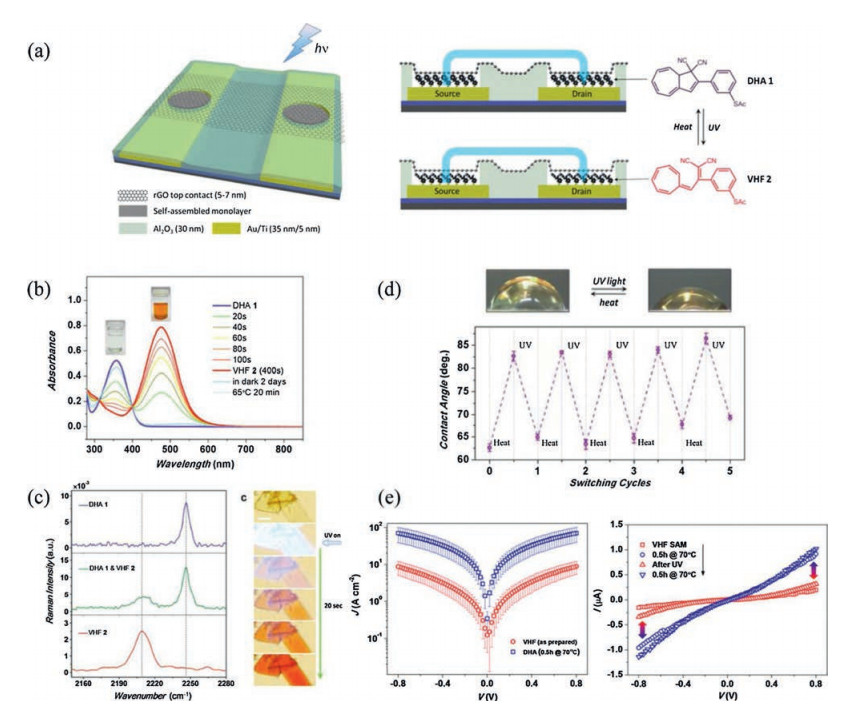
Utilizing rGO films as soft top-contacts, we constructed lightswitchable solid-state molecular junctions based on DHA/VHF molecules (Fig. 3) [22]. Due to the high transparency (up to 90%), superior flexibility and conductivity of rGO films, the DHA/VHF molecules in junctions can be photo-induced in situ, and the electrical properties of them could also be measured simultaneously. Experimental results showed that the conductivity of DHA-based SAMs is higher than that of VHF-based SAMs due to a more uniform conformation of DHA molecules in the SAM. By alternating thermal annealing and UV irradiation, bidirectional switches with an average current on/off ratio of 5-7 could be obtained. Further control experiments revealed that the switching properties were dominated by the intrinsic properties of DHA/VHF molecules.

|
Download:
|
| Fig. 3. Light switchable solid-state molecular junctions with rGO thin films as transparent top-contacts. (a) Schematic view of molecular test bed with rGO thin film as transparent top-contact and schematic cross section of the molecular junction and molecular structure of DHA 1 and VHF 2 illustrating the thermo-optical switching. (b) UVvis absorption spectroscopy of DHA 1 and VHF 2 in MeCN. (c) Raman spectra of solid-state powders composed of DHA 1 only, a mixture of DHA 1 and VHF 2, and VHF 2 only. (d) Optical images of water droplets on surface of DHA 1 (left) and VHF 2 (right) SAMs, and reversible wettability transitions as a function of alternating thermal treatment and UV irradiation. (e) J-V characteristics of VHF 2 (as prepared) and DHA 1 (70 ℃ for 0.5 h) isomers self-assembled in the molecular junctions (left), and conductance on/off ratio histogram (purple bars) based on more than 200 junctions (right). Adapted with permission [22]. Copyright 2013, Wiley-VCH. | |
4.2. π-Conjugated polymers
Although conjugated polymers (CPs) and their bulk applications in optoelectronics have received significant attention for decades [71], very limited work has been carried out on incorporating CPs into molecular-scale electronics. Compared with small molecules, CPshave complex interchain interactions, long lengths and unclear charge transport mechanisms over long pathways [72, 73]. Recently some progress in CP-based molecular electronics have been achieved. For vertical junctions, polymeric SAMs were usually obtained in situ by sequential stepwise addition-or coordination-reaction [74, 75]. For planner junctions, polymerization via electro-oxidation of thiophene [76, 77], pyrrole [78, 79] and aniline [80] by conducting atomic force microscopy is usually adopted. Moreover, thiophene-Au interaction [81-84] and salt formation of polypyrrole [85] can also be used to form CPbased planar molecular junctions.
Poly(p-phenyleneethynylene)s (PPEs) have been widely studied in organic electronics [86]. Hu et al. reported self-assembled nanojunctions based on TA-PPE (PPEs derivatives modified with thioacetyl end group) [87]. The nanojunctions could act as nanoscale photoswitches under photoirradiation. To understand the electron transport in the TA-PPE junctions, they further examined two possible mechanisms for the polymer molecular junctions [88]. First-principles calculations revealed that the opening of different conducting channels led to the highly periodic and identical stepwise features. Further, Dong et al. fabricated photoswitching devices of TA-PPE films prepared on poly(tetrafluoroethylene) (PTFE) substrate by friction transfer technique [89]. CPs with alignment had an on/off ratio 330-400, while that without alignment only had an on/off ratio 8-12. The dramatic differences revealed the efficient charge transfer in the aligned TAPPE films. In addition, they grew highly crystalline nanowires of TA-PPE and fabricated organic field-effect transistors (OFETs) [90]. The transistors showed an average charge carrier mobility of ~10-2 cm2 V-1 s-1 and a highest mobility of 0.1 cm2 V-1 s-1.
By incorporating TTF units into the backbone of PPEs, we reported a novel type of molecular tunneling junction based on ultrathin films of TTF-PPEs and investigated their electrical properties (Fig. 4) [71]. Modified with anchoring group (thioacetyl group, -SCOCH3) on both ends of the polymer terminal, TTF-PPEs can bond to the Au surface in a self-assembly manner. Experimental results showed that the SAM of TTF-PPEs was in a planar manner on Au surface rather than a vertically oriented manner like small molecules monolayer. By transferring a solution-processed reduced graphene oxide (rGO) film (5-7 nm) as soft top-contact, molecular junctions were constructed with high yield and operational stability. Electrical measurements of devices showed that adding TTF units into PPEs backbone could decrease the energy gap and improve the alignment of energy level to Au. In addition, the electronic properties of TTF-PPE junctions could be easily modulated via an electrochemical method. These results demonstrated the potential of CPs as an alternative for the construction of molecular electronic devices.

|
Download:
|
| Fig. 4. rGO test bed with self-assembled CPs on Au bottom electrode. (a) Chemical structure of PPE and TTF-PPE. (b) Cyclic voltammograms of PPEs and TTF-PPEs dissolved in tetrahydrofuran solution. (c) Optical images depicting the process of device fabrication using thin Au film as masks to remove the unwanted parts of rGO films. (d) Schematic view of rGO top-contact test bed for molecular tunneling junctions. The blue arrow in (d) indicates charge transfer between adjacent junctions via graphene top contact. (e) Schematic view of self-assembled small molecules and long CPs inside in junctions. The blue arrows in (e) indicate charge transfer by direct tunneling across the molecular barriers. Reprinting with permission [71]. Copyright 2015, Nature Publishing Group. | |
5. Summary and outlook
Molecular electronics has achieved great progress in recent years. Device fabrication and functionality are two crucial aspects and still main challenges in this field. To effectively and conveniently construct molecular-scale devices, developing advanced fabrication techniques is important. Though various techniques/methods have been developed, there is still no consensus on a standard route to device fabrication. On the other hand, to endow molecular-scale devices with more functions, more efforts should be devoted to molecular design and synthesis to meet the increasing demands of practical applications. From fabrication to functionality, there is still a long way for molecularscale electronics to explore in the future.
AcknowledgmentsThe authors acknowledge financial support from the National Natural Science Foundation of China (No. 51673114), Shanghai Science and Technology Committee (No. 17ZR1447300) and Basic Research Development Programme (No. 2017YFA0207500).
| [1] |
A. Aviram, M.A. Ratner, Chem. Phys. Lett. 29(1974) 277-283. DOI:10.1016/0009-2614(74)85031-1 |
| [2] |
G.E. Moore, Electronics 38(1965) 114. |
| [3] |
S. Reineke, F. Lindner, G. Schwartz, et al., Nature 459(2009) 234-238. DOI:10.1038/nature08003 |
| [4] |
C. Wang, H. Dong, W. Hu, Y. Liu, D. Zhu, Chem. Rev. 112(2012) 2208-2267. DOI:10.1021/cr100380z |
| [5] |
Y. Lin, Y. Li, X. Zhan, Chem. Soc. Rev. 41(2012) 4245-4272. DOI:10.1039/c2cs15313k |
| [6] |
D. Xiang, X. Wang, C. Jia, T. Lee, X. Guo, Chem. Rev. 116(2016) 4318-4440. DOI:10.1021/acs.chemrev.5b00680 |
| [7] |
B. Mann, H. Kuhn, J. Appl. Phys. 42(1971) 4398-4405. DOI:10.1063/1.1659785 |
| [8] |
B. Xu, N.J. Tao, Science 301(2003) 1221-1223. DOI:10.1126/science.1087481 |
| [9] |
C. Huang, A.V. Rudnev, W. Hong, T. Wandlowski, Chem. Soc. Rev. 44(2015) 889-901. DOI:10.1039/C4CS00242C |
| [10] |
L.J. Wang, K.G. Zhou, L. Tan, et al., Chem. Eur. J. 17(2011) 8414-8423. DOI:10.1002/chem.201003507 |
| [11] |
L.J. Wang, A. Yong, K.G. Zhou, et al., Chem. Asian J. 8(2013) 1901-1909. DOI:10.1002/asia.v8.8 |
| [12] |
M.A. Reed, Science 278(1997) 252-254. DOI:10.1126/science.278.5336.252 |
| [13] |
D. Xiang, H. Jeong, T. Lee, D. Mayer, Adv. Mater. 25(2013) 4845-4867. DOI:10.1002/adma.201301589 |
| [14] |
C. Huang, M. Jevric, A. Borges, et al., Nat. Commun. 8(2017) 15436. DOI:10.1038/ncomms15436 |
| [15] |
T. Li, W. Hu, D. Zhu, Adv. Mater. 22(2010) 286-300. DOI:10.1002/adma.v22:2 |
| [16] |
R.M. Metzger, B. Chen, U. Höpfner, et al., J. Am. Chem. Soc. 119(1997) 10455-10466. DOI:10.1021/ja971811e |
| [17] |
A.A. Kornyshev, A.M. Kuznetsov, J. Ulstrup, Proc. Natl. Acad. Sci. U. S. A. 103(2006) 6799-6804. DOI:10.1073/pnas.0511188103 |
| [18] |
C.P. Collier, Science 289(2000) 1172-1175. DOI:10.1126/science.289.5482.1172 |
| [19] |
C. Jia, A. Migliore, N. Xin, et al., Science 352(2016) 1443-1445. DOI:10.1126/science.aaf6298 |
| [20] |
A.S. Blum, J.G. Kushmerick, D.P. Long, et al., Nat. Mater. 4(2005) 167-172. DOI:10.1038/nmat1309 |
| [21] |
S.W. Lee, S.J. Park, E.E.B. Campbell, Y.W. Park, Nat. Commun. 2(2011) 220. DOI:10.1038/ncomms1227 |
| [22] |
T. Li, M. Jevric, J.R. Hauptmann, et al., Adv. Mater. 25(2013) 4164-4170. DOI:10.1002/adma.201300607 |
| [23] |
J.O. Lee, Y.H. Song, M.W. Kim, et al., Nat. Nanotechnol. 8(2012) 36-40. |
| [24] |
P.L. McEuen, H. Park, J. Park, et al., Nature 407(2000) 57-60. DOI:10.1038/35024031 |
| [25] |
S. Kubatkin, A. Danilov, M. Hjort, et al., Nature 425(2003) 698-701. DOI:10.1038/nature02010 |
| [26] |
S.V. Aradhya, L. Venkataraman, Nat. Nanotechnol. 8(2013) 399-410. DOI:10.1038/nnano.2013.91 |
| [27] |
H. Haick, D. Cahen, Acc. Chem. Res. 41(2008) 359-366. DOI:10.1021/ar700099n |
| [28] |
W. Hong, D.Z. Manrique, P. Moreno-García, et al., J. Am. Chem. Soc. 134(2012) 2292-2304. DOI:10.1021/ja209844r |
| [29] |
J. Xiang, B. Liu, S.T. Wu, et al., Angew. Chem. Int. Ed. 44(2005) 1265-1268. DOI:10.1002/(ISSN)1521-3773 |
| [30] |
H. Park, A.K.L. Lim, A.P. Alivisatos, J. Park, P.L. McEuen, Appl. Phys. Lett. 75(1999) 301-303. DOI:10.1063/1.124354 |
| [31] |
W. Chen, H. Ahmed, K. Nakazoto, Appl. Phys. Lett. 66(1995) 3383-3384. DOI:10.1063/1.113765 |
| [32] |
T. Nagase, T. Kubota, S. Mashiko, Thin Solid Films 438(2003) 374-377. |
| [33] |
T. Li, W. Hu, Nanoscale 3(2011) 166-176. DOI:10.1039/C0NR00325E |
| [34] |
T. Li, L. Su, W. Hu, et al., Anal. Chem. 82(2010) 1521-1526. DOI:10.1021/ac902681g |
| [35] |
T. Li, H. Dong, X. Fu, et al., Small 10(2014) 878-883. DOI:10.1002/smll.201300656 |
| [36] |
M.T. Dang, L. Hirsch, G. Wantz, Adv. Mater. 23(2011) 3597-3602. DOI:10.1002/adma.201100792 |
| [37] |
H. Zhu, T. Li, Y. Zhang, et al., Adv. Mater. 22(2010) 1645-1648. DOI:10.1002/adma.200903671 |
| [38] |
K.S. Novoselov, A.K. Geim, S.V. Morozov, et al., Science 306(2004) 666-669. DOI:10.1126/science.1102896 |
| [39] |
F. Prins, A. Barreiro, J.W. Ruitenberg, et al., Nano Lett. 11(2011) 4607-4611. DOI:10.1021/nl202065x |
| [40] |
Y. Cao, S. Dong, S. Liu, et al., Angew. Chem. Int. Ed. 51(2012) 12228-12232. DOI:10.1002/anie.v51.49 |
| [41] |
Y. He, H. Dong, T. Li, et al., Appl. Phys. Lett. 97(2010) 133301-133303. DOI:10.1063/1.3493647 |
| [42] |
U.C. Fischer, H.P. Zingsheim, J. Vac. Sci. Technol. 19(1981) 881-885. DOI:10.1116/1.571227 |
| [43] |
P. Colson, C. Henrist, R. Cloots, J. Nanomater. 2013(2013) 1-19. |
| [44] |
D. Ji, T. Li, H. Fuchs, Adv. Electron. Mater. 3(2017) 1600348. DOI:10.1002/aelm.201600348 |
| [45] |
S. Casalini, C.A. Bortolotti, F. Leonardi, F. Biscarini, Chem. Soc. Rev. 46(2017) 40-71. DOI:10.1039/C6CS00509H |
| [46] |
C.R. Hansen, T.J. Sørensen, M. Glyvradal, et al., Nano Lett. 9(2009) 1052-1057. DOI:10.1021/nl803393m |
| [47] |
Y.L. Loo, D.V. Lang, J.A. Rogers, J.W.P. Hsu, Nano Lett. 3(2003) 913-917. DOI:10.1021/nl034207c |
| [48] |
A. Vilan, D. Cahen, Adv. Funct. Mater. 12(2002) 795-807. DOI:10.1002/adfm.200290009 |
| [49] |
K.T. Shimizu, J.D. Fabbri, J.J. Jelincic, N.A. Melosh, Adv. Mater. 18(2006) 1499-1504. DOI:10.1002/(ISSN)1521-4095 |
| [50] |
M.L. Chabinyc, X. Chen, R.E. Holmlin, et al., J. Am. Chem. Soc. 124(2002) 11730-11736. DOI:10.1021/ja020506c |
| [51] |
M.M. Thuo, W.F. Reus, C.A. Nijhuis, et al., J. Am. Chem. Soc. 133(2011) 2962-2975. DOI:10.1021/ja1090436 |
| [52] |
J.K.N. Mbindyo, T.E. Mallouk, J.B. Mattzela, et al., J. Am. Chem. Soc. 124(2002) 4020-4026. DOI:10.1021/ja016696t |
| [53] |
H.B. Akkerman, P.W.M. Blom, D.M. de Leeuw, B. deBoer, Nature 441(2006) 69-72. DOI:10.1038/nature04699 |
| [54] |
G. Wang, Y. Kim, M. Choe, T.W. Kim, T. Lee, Adv. Mater. 23(2010) 755-760. |
| [55] |
T. Li, J.R. Hauptmann, Z. Wei, et al., Adv. Mater. 24(2012) 1333-1339. DOI:10.1002/adma.201104550 |
| [56] |
J.R. Hauptmann, T. Li, S. Petersen, et al., Phys. Chem. Chem. Phys. 14(2012) 14277-14281. DOI:10.1039/c2cp41723e |
| [57] |
V. Ferri, M. Elbing, G. Pace, et al., Angew. Chem. 120(2008) 3455-3457. DOI:10.1002/(ISSN)1521-3757 |
| [58] |
S.D. Evans, S.R. Johnson, H. Ringsdorf, L.M. Williams, H. Wolf, Langmuir 14(1998) 6436-6440. DOI:10.1021/la980450t |
| [59] |
J.M. Mativetsky, G. Pace, M. Elbing, et al., J. Am. Chem. Soc. 130(2008) 9192-9193. DOI:10.1021/ja8018093 |
| [60] |
A.S. Kumar, T. Ye, T. Takami, et al., Nano Lett. 8(2008) 1644-1648. DOI:10.1021/nl080323+ |
| [61] |
A.C. Whalley, M.L. Steigerwald, X. Guo, C. Nuckolls, J. Am. Chem. Soc. 129(2007) 12590-12591. DOI:10.1021/ja073127y |
| [62] |
N. Katsonis, T. Kudernac, M. Walko, et al., Adv. Mater. 18(2006) 1397-1400. DOI:10.1002/(ISSN)1521-4095 |
| [63] |
A.J. Kronemeijer, H.B. Akkerman, T. Kudernac, et al., Adv. Mater. 20(2008) 1467-1473. DOI:10.1002/(ISSN)1521-4095 |
| [64] |
X. Guo, L. Huang, S. O'Brien, P. Kim, C. Nuckolls, J. Am. Chem. Soc. 127(2005) 15045-15047. DOI:10.1021/ja054335y |
| [65] |
G. Berkovic, V. Krongauz, V. Weiss, Chem. Rev. 100(2000) 1741-1754. DOI:10.1021/cr9800715 |
| [66] |
J. Daub, T. Knöchel, A. Mannschreck, Angew. Chem. Int. Ed.Engl. 23(1984) 960-961. DOI:10.1002/(ISSN)1521-3773 |
| [67] |
J.X. Dong, H.L. Zhang, Chin. Chem. Lett. 27(2016) 1097-1104. DOI:10.1016/j.cclet.2016.05.005 |
| [68] |
S. Lara-Avila, A.V. Danilov, S.E. Kubatkin, et al., J. Phys. Chem. C 115(2011) 18372-18377. DOI:10.1021/jp205638b |
| [69] |
S.L. Broman, S. Lara-Avila, C.L. Thisted, et al., Adv. Funct.Mater. 22(2012) 4249-4258. DOI:10.1002/adfm.v22.20 |
| [70] |
B.K. Pathem, Y.B. Zheng, S. Morton, et al., Nano Lett. 13(2013) 337-343. DOI:10.1021/nl304102n |
| [71] |
Z. Wang, H. Dong, T. Li, et al., Nat. Commun. 6(2015) 7478. DOI:10.1038/ncomms8478 |
| [72] |
H. Dong, W. Hu, Acc. Chem. Res. 49(2016) 2435-2443. DOI:10.1021/acs.accounts.6b00368 |
| [73] |
Z.Y. Zhang, T. Li, Chin. Chem. Lett. 27(2016) 1209-1222. DOI:10.1016/j.cclet.2016.05.031 |
| [74] |
S.H. Choi, C.D. Frisbie, J. Am. Chem. Soc. 132(2010) 16191-16201. DOI:10.1021/ja1060142 |
| [75] |
N. Tuccitto, V. Ferri, M. Cavazzini, et al., Nat. Mater. 8(2008) 41-46. |
| [76] |
A. Berlin, G. Zotti, G. Schiavon, S. Zecchin, J. Am. Chem. Soc. 120(1998) 13453-13460. DOI:10.1021/ja9824728 |
| [77] |
M.N.O. afrain, T.K. Tran, P. Blanchard, et al., Adv. Funct. Mater 18(2008) 2163-2171. DOI:10.1002/adfm.v18:15 |
| [78] |
R.L. McCarley, R.J. Willicut, J. Am. Chem. Soc. 120(1998) 9296-9304. DOI:10.1021/ja981677d |
| [79] |
J.S. Lee, Y.S. Chi, I.S. Choi, J. Kim, Langmuir 28(2012) 14496-14501. DOI:10.1021/la302526t |
| [80] |
S. Kuwabata, R. Fukuzaki, M. Nishizawa, C.R. Martin, H. Yoneyama, Langmuir 15(1999) 6807-6812. DOI:10.1021/la981719b |
| [81] |
Z. Gao, K.S. Siow, H.S.O. Chan, Synthetic Met. 75(1995) 5-10. DOI:10.1016/0379-6779(95)03384-V |
| [82] |
Z. Gao, K.S. Siow, Electrochim. Acta. 42(1997) 315-321. DOI:10.1016/0013-4686(96)00187-9 |
| [83] |
D. Yang, M. Zi, B. Chen, Z. Gao, J. Electroanal. Chem. 470(1999) 114-119. DOI:10.1016/S0022-0728(99)00216-8 |
| [84] |
Y. Shimoyama, Thin Solid Films 464-465(2004) 403-407. DOI:10.1016/j.tsf.2004.06.003 |
| [85] |
B. Vercelli, G. Zotti, A. Berlin, S. Grimoldi, Chem. Mater. 18(2006) 3754-3763. DOI:10.1021/cm060802e |
| [86] |
U.H.F. Bunz, Chem. Rev. 100(2000) 1605-1644. DOI:10.1021/cr990257j |
| [87] |
W. Hu, H. Nakashima, K. Furukawa, et al., J. Am. Chem. Soc. 127(2005) 2804-2805. DOI:10.1021/ja0433929 |
| [88] |
W. Hu, J. Jiang, H. Nakashima, et al., Phys. Rev. Lett. 96(2006) 027801-027803. DOI:10.1103/PhysRevLett.96.027801 |
| [89] |
H. Dong, H. Li, E. Wang, et al., Langmuir 24(2008) 13241-13244. DOI:10.1021/la8026094 |
| [90] |
H. Dong, S. Jiang, L. Jiang, et al., J. Am. Chem. Soc. 131(2009) 17315-17320. DOI:10.1021/ja907015p |