 2017, Vol. 28


b Department of Polymer Engineering, College of Polymer Science and Polymer Engineering, The University of Akron, Akron, OH 44325, USA
Bulk heterojunction (BHJ) polymer solar cells (PSCs) have attracted tremendous attention due to its intrinsic merits of lowcost, flexibility and the possibility of high throughput manufacturing [1–3]. So far, tremendous efforts including development of novel narrow band-gap conjugated polymers with high charge carrier mobility [4], unique edge-on molecular packing patterns [5] and interfacial reengineering of PSCs [6–8] via functional buffer layers, have been devoted to boost the power conversion efficiencies (PCEs) of PSCs. PCEs over 10% from single-junction PSCs with a conventional device structure have been reported [9]. Nevertheless, the conventional structured PSCs with commonly used poly(3, 4-ethylenedioxythiophene) polystyrene sulfonate (PEDOT:PSS) interface layer suffered low device stability due to the acidic nature of PEDOT:PSS anode buffer layer [10]. In addition, the air-sensitive lowwork-function metal cathode (Al) in the conventional structured PSCs will further deteriorate the device stability. Such low stability issues are predominant obstacles for PSCs' commercialization. Hereupon, an inverted PSCs (i-PSCs) with air-stable high-workfunction metals as the anode (Ag or Au) [11–13] and robust electrode buffer layers are ideal alternatives. However, the commonly used ZnO [13–15] electron extraction layer (EEL) in the i-PSCs was required high temperature annealing (>500 ℃) processing, which was incompatible with the flexible substrates and low-cost processing requirements. In addition, the residual organic compounds as well as the grain boundaries from the poorly crystallization in solutionprocess ZnO EEL would also raise the series resistance, decrementing charge transport [13, 16, 17]. And the inhomogeneity of the ZnO film induced by the wide ZnO nanoparticles (NPs) size-distribution would also cause the lateral current flow and low photocurrent. Therefore, it is of great importance to develop an easy solution-processed, high quality, homogeneous, and large band-gap materials as the EEL for approaching efficient and stable i-PSCs.
A ternary semiconductor Zn2SnO4 (ZSO), which possesses high electron mobility and electrical conductivity, and high transparency in visible range, has been widely used as gas sensors [18, 19], Li+ battery electrodes [20, 21], and organ-degradation photocatalysts [22–24]. Moreover, the mutinary ZSO, as compared with simple binary ZnO, are expected to have higher possibility for tuning its electrical and optical properties. Thus, in this study, we report lowtemperature solution-processed narrow-size-distributed ZSO NPs as the EEL in the i-PSCs. Furthermore, poly[(9, 9-bis(30-(N, N-dimethylamino)propyl)-2, 7-fluorene)-alt-2, 7-(9, 9-dioctylfluorene)] (PFN) is used to modify the surface properties of ZSO thin film. By using the ZSO NPs/PFN as the EEL, the i-PSCs fabricated by poly[4, 8-bis(2-ethylhexyloxyl)benzo[1, 2-b:4, 5-b’]dithio-phene-2, 6-diyl-altethylhexyl-3-fluorothithieno [3, 4-b]thiophene-2-carboxylate-4, 6-diyl] (PTB7) blended with (6, 6)-phenyl-C71-butyric acid methyl ester (PC71BM) BHJ composite exhibits a PCE of 8.44%, which is nearly 10% enhancement as compared with that of 7.75% observed from the i-PSCs by PTB7:PC71BM BHJ composite using the ZnO/PFN EEL.
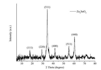
2. Results and discussionFig. 1 presents the XRD pattern of ZSO powder. The diffraction peaks centered at 2θ of 17.88, 29.28, 34.48, 41.78, 55.18, and 60.38 are corresponding to the (111), (220), (311), (400), (511) and (440) planes of ZSO crystals. No impurity peak is found in the XRD spectrum of ZSO, which indicates that highly purified ZSO NPs is synthesized by low-temperature hydrothermal route. According to the Scherrer equation [25], the average size of ZSO NPs is estimated to be about 14 nm.

|
Download:
|
| Fig. 1. The XRD pattern of ZSO NPs | |
The TEM image of ZSO is shown in Fig. 2a. It is clearly that ZSO NPs exhibits good size-distribution. The relative small particle size and narrow size-distribution are favorable for forming homogeneous film which is critical for minimizing linkage current in solar cells. In addition, the high-resolution TEM image (Fig. 2b) and the SAED pattern (Fig. 2c) are in good agreement with the spinel structure of ZSO deduced from XRD pattern.

|
Download:
|
| Fig. 2. (a) The TEM image of ZSO NPs, (b) high-resolution TEM and (c) SAED pattern of ZSO NPs | |
The surface root-mean-square roughness (RMS) measured by AFM. As shown in Fig. 3. The RMS is 5.95 nm for ZSO NPs thin film and 1.09 nm for ZnO. In addition, the particle-featured morphology of ZSO NPs film easily forms surface defects. The defective surface of the ZSO EEL would be harmful to the electron being extracted from BHJ active layer to ITO cathode [3, 26], resulting in charge carrier accumulation and recombination. In order to overcome this problem, PFN is used to reengineering the surface of the ZnO and ZSO EELs for facilitating the electron extraction. After modifying the surface of ZSO NPs and ZnO by PFN, the RMS is 6.25 nm for the ZSO/PFN thin film and 1.09 nm for the ZnO/PFN thin film. Since the PFN layer is very thin and PFN is easily to be aggregated, the ultrathin PFN layer could not incompletely cover the rough ZSO NPs film. Slightly larger RMS of the ZSO/PFN thin film is observed as compared with ZSO thin films [3].

|
Download:
|
| Fig. 3. AFM tapping-mode image of (a) ZnO (RMS of 1.09 nm), (b) ZSO NPs (RMS of 5.95 nm), (c) ZnO/PFN (RMS of 0.96 nm) and (d) ZSO/PFN (RMS of 6.25 nm) thin film | |
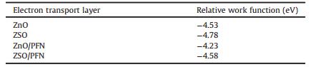
The work functions (WF) of ZnO, ZSO, ZnO/PFN and ZSO/PFN thin films were estimated by Scanning Kelvin Probe measurement. The results are summarized in Table 1. The WF of ZSO NPs thin film is -4.78 eV, which is higher than that (-4.53 eV) of ZnO thin film. As expected, reduced WFs of -4.23 eV and -4.58 eV are observed from the ZnO/PFN thin film and the ZSO/PFN thin film, respectively.
|
|
Table 1 Relative work functions of different electron extraction layers |
The device structure of the i-PSCs with ZnO, ZnO/PFN, ZSO NPs and ZSO NPs/PFN EELs are shown in Scheme 1a. The molecular structures of PTB7, PC71BM and PFN are shown in Scheme 1b. Based on the estimated WFs of different EELs, the WFs of ITO and Ag electrodes, the lowest unoccupied molecular orbital (LUMO) and highest occupied molecular orbital (HOMO) energy levels of PTB7, PC71BM and MoO3, and the schematic energy diagram of the i-PSCs with different EELs are shown in Scheme 1c. The low-lying WF of the ZSO/PFN thin film is favorable for separated electrons to be extracted from BHJ active layer to ITO cathode. Thus, high device performance is expected from the i-PSCs incorporated with the ZSO/PFN EEL.

|
Download:
|
| Scheme1. (a) Schematic illustration of the inverted device architecture with different EELs; (b) molecular structures of PTB7, PC71BM, and PFN and (c) schematic energy diagrams of the i-PSCs with different EELs | |
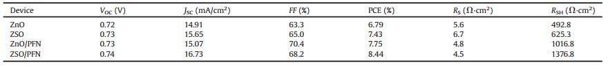
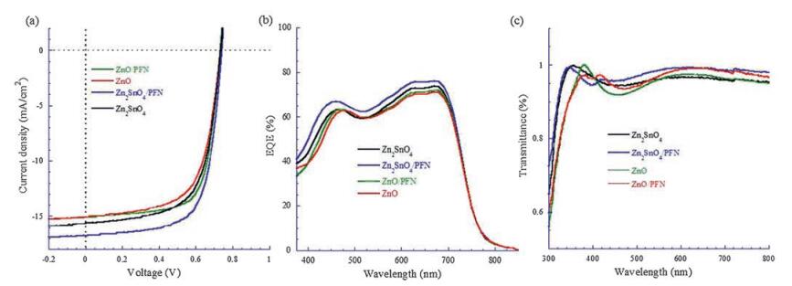
The current density–voltage (J–V) characteristics of the i-PSCs under AM 1.5 G solar illumination (100 mW/cm2) are shown in Fig. 4a and the photovoltaic parameters are summarized in Table 2. The i-PSC with the ZnO EEL exhibits an open-circuit voltage (VOC) of 0.72 V, a short-circuit current (JSC) of 14.91 mA/cm2, and a fill factor (FF) of 63.3%, with a corresponding PCE of 6.79%. The i-PSC with the ZnO/PFN EEL exhibits a VOC of 0.73 V, a JSC of 15.07 mA/cm2 and an FF of 70.4%, with a corresponding PCE of 7.75%. Under the same illumination condition, the i-PSC with the ZSO NPs EEL exhibits a VOC of 0.73 V, a JSC of 15.65 mA/cm2 and an FF of 65.0%, with a corresponding PCE of 7.43%, and the i-PSC with the ZSO/PFN EEL exhibits a VOC of 0.74 V, a JSC of 16.73 mA/cm2 and an FF of 68.2%, with a corresponding PCE of 8.44%. It is clearly that the i-PSCs incorporated with either ZnO/PFN or ZSO/PFN EEL possess better device performance than those incorporated with pure ZnO or ZSO EELs. Moreover, the enhanced PCE of the i-PSC with the ZSO/PFN EEL, as compared with the i-PSC with the ZnO/PFN EEL, is mainly attributed to enlarged JSC, which shows an augment from 15.65 to 16.73 mA/cm2. The increased JSC is further evidenced in the EQE measurement, as shown in Fig. 4b. Integration of the EQE spectra over the wavelength ranging from 375 to 800 nm affords the photocurrent of 14.39, 14.50, 14.93 and 15.59 mA/cm2 for the i-PSCs incorporated with ZnO EEL, ZnO/PFN EEL, ZSO EEL and ZSO/PFN EEL, respectively. These integrated JSC values are in good agreement with the JSC values observed from the J-V characteristics (Fig. 4a).

|
Download:
|
| Fig. 4. (a) J–V characteristics (under illumination, AM 1.5 G, 100 mW/cm2); (b) external quantum efficiency (EQE) of i-PSCs with ZnO, ZnO/PFN, ZSO and ZSO/PFN EEL, and (c) optical transparency as a function of wavelength (λ) of ZnO, ZnO/PFN, ZSO and ZSO/PFN film | |
|
|
Table 2 Device performance including series resistance (RS) and shunt resistance (RSH) based on PTB7:PC71BM under 100 mW/cm2 AM illumination with various inter layers |
In order to understand enlarged JSC from the i-PSCs incorporated with the ZSO/PFN EEL, the transmittance spectra of ZnO, ZSO, ZnO/PFN and ZSO/PFN were measured. The results are shown in Fig. 4c. The enhanced transmittance of ZSO NPs and ZSO/PFN thin films in the visible range, would allow more photons to be absorbed by BHJ active layer, generating more charge carrier, consequently, high JSC.
The I–V characteristics of ITO/ZnO(ZnO/PFN, ZSO, ZSO/PFN) (40 nm)/Ag devices, measured in dark, are shown in Fig. 5a. From the slope of I–V plot, the direct current conductivity (δ), described as I = δA d-1 V, where A is the area (0.057 cm2) and d is the thickness of sample (40 nm), can be estimated. High electrical conductivity ZSO would facilitate the i-PSCs incorporated with the ZSO EEL or the ZSO/PFN EEL to reduce charge carrier recombination. As a result, the increased JSC, as anticipated, are observed from the i-PSCs incorporated with ZSO EEL or ZSO/PFN EEL.

|
Download:
|
| Fig. 5. (a) The I–V plots of ITO/ZnO (ZnO/PFN, ZSO or ZSO/PFN) (40 nm)/Ag devices in dark and (b) J–V characteristics of the i-PSCs with ZnO, ZnO/PFN, ZSO and ZSO/PFN EELs measured in dark | |
The improved VOC of the i-PSCs with the ZSO NPs/PFN or the ZnO/PFN EEL are originated from that the PFN interlayer reduces the WF of the ZSO NPs EEL or the ZnO EEL and thus form a better energy level alignment between the cathode and active layer. The i-PSC incorporated with ZSO/PFN EEL possessed higher shunt resistances (RSH), derived from the J–V curves, than that incorporated with ZnO/PFN EEL. Higher RSH, which means less linkage current (as shown in Fig. 5b), contributes to the slightly higher VOC of the ZSO/PFN-based i-PSC. The FF of the i-PSCs with the ZnO/PFN or the ZSO/PFN EELs is also enhanced as compared with the i-PSCs with solo EEL. The enhanced interfacial contact (from organic–inorganic contact for ZnO or ZSO NPs/active layer to organic–organic contact for PFN/active layer) facilitates the electron extraction and avoids the electron accumulation near the interlayer, resulting in high FF [3].
3. ConclusionIn conclusion, we have successfully synthesized Zn2SnO4 nanoparticles with a narrow size distribution (~14 nm) by a facile hydrothermal route under 100 ℃. By employing PFN interlayer to modify the ZSO and ZnO surface, simultaneously increased photovoltaic parameters (VOC, JSC and FF) are observed from polymer solar cells with an inverted device structure (i-PSCs). The improvement is originating from improved interfacial contact with active layer and the better energy level alignment between active layer and electrode. The JSC of the i-PSC with ZSO/PFN EEL is dramatically enhanced after PFN modifying the defective ZSO surface. Consequently, i-PSCs with the ZSO/PFN EEL exhibit a PCE of 8.44%, which is nearly 10% enhancement as compared with that of 7.75% observed from i-PSCs with the ZnO/PFN EEL.
4. Experimental 4.1. MaterialsBoth PTB7 and PC71BM were purchased from 1-Material Inc. and used as received without further purification. Zinc chloride, tin(Ⅳ) chloride pentahydrate, zinc acetate dehydrate and all other reagents were purchased from Sigma Aldrich. PFN was synthesized in our laboratory [27].
4.2. Preparation of ZSO NPs and ZnO precursor solutionZSO NPs were synthesized by the sol-gel process based on the reported method [28]. ZnCl2 (1.2 mmol) and SnCl4·5H2O (0.6 mmol) were dissolved in deionized water (15 mL) under vigorous magnetic stirring for 15 min. 9.6 mmol N2H4·H2O was then added to the reaction solution under vigorous magnetic stirring. After stirring for 30 min, the obtained suspension was transferred into a 30 mL autoclave and then heated statically at 100 ℃ for 12 h. The obtained products were thoroughly washed with deionized water and ethanol, and then dispersed in 2-methoxy ethanol to result in a colloidal solution.
For compassion studies, ZnO precursor was also prepared by dissolving 1.0 g zinc acetate dihydrate (Zn(CH3COO)2·2H2O) and 0.28 g ethanolamine (NH2CH2CH2OH) in 10 mL 2-methoxyethanol (CH3OCH2CH2OH) under vigorous stirring for the hydrolysis reaction (12 h).
4.3. Characterization of ZSO NPsThe crystal structure and phase of ZSO NPs were characterized by X-ray diffraction (XRD) measurement on X'Pert Pro. The film morphologies and film microstructures were investigated by transmission electron microscopy (TEM) on JEOL JEM-2100F and atomic force microscopy (AFM) on Bruker multimode 8. Thin film absorption spectra were conducted on the HP 8453 spectrophotometer. The work functions of thin films were estimated by the Scanning Kelvin Probe measurement (SKP 5050, KP Technology).
4.4. The i-PSCs fabricationFor compassion studies, ZnO, ZnO/PFN, ZSO NPs and ZSO ZSO NPs/PFN thin film layers were used as the EELs in the i-PSCs with a device structure of ITO/EELs/PTB7:PC71BM/MoO3/Ag, where ITO is indium tin oxide and Ag is sliver. About 35 nm ZnO thin was spincoated on the pre-cleaned ITO glass substrates from ZnO precursor solution, followed with thermal annealing at 200 ℃ for 1 h. About 35 nm ZSO NPs thin film was prepared by spin-coating ZSO NPs dispersion onto the pre-cleaned ITO glass substrates at 3000 rpm for 30 s, followed by thermal annealing at 100 ℃ for 1 h. To obtain ZnO/PFN and ZSO NPs/PFN EELs, about 5 nm PFN thin film was deposited on either ZnO or ZSO NPs thin films from methanol solution (0.5 mg/mL). Afterwards, an about 90 nm BHJ composite was spin-coated on the top of above EELs from the chlorobenzene solution composing of PTB7 and PC71BM (1:1.5 by weight, a polymer concentration of 9.0 mg/mL), with 3% (v/v) 1, 8-diiodooctane (DIO) in the glove box under nitrogen atmosphere. The casted film was kept in a low pressure environment of 10–1 bar for 6 h. After that, an about 10 nm MoO3 layer and about 100 nm Ag electrode were thermally sequentially evaporated in vacuum with a base pressure of 2.0 × 10⁻⁴ Pa. The device area was measured to be 16 mm2.
4.5. Characterization of the i-PSCsThe current density versus voltage (J–V) characteristics of the iPSCs were measured on Keithley 2400 source meter under 1 sun, AM 1.5 G spectrum from a solar simulator (Japan, SAN-EI, XES-40S1) with the light intensity of 100 mW/cm2. The light intensity was calibrated by a Newport certified reference silicon cell (PV Measurements, with KG-5 visible filter). Spectral mismatch factors (M) value of 1.03 was used to obtain the correct photocurrent and efficiency for the devices according to previously published paper [29], where the measurement condition are identical.
AcknowledgmentThis work was supported by National Natural Science Foundation of China (No. 51329301).
| [1] | S.G. Benka. The energy challenge. Physics Today 55 (2002) 38–39. |
| [2] | H. Youn, H.J. Park, L.J. Guo. Organic photovoltaic cells:from performance improvement to manufacturing processes. Small 11 (2015) 2228–2246. DOI:10.1002/smll.v11.19 |
| [3] | C. Han, Y. Cheng, L. Chen L, et al., Enhanced performance of inverted polymer solar cells by combining ZnO nanoparticles and poly (9, 9-bis(3'-(N, N-dimethylamino)propyl)-2, 7-fluorene)-alt-2, 7-(9, 9-dioctyfluorene) as electron transport layer. ACS Appl. Mater. Int. 8 (2016) 3301–3307. DOI:10.1021/acsami.5b11140 |
| [4] | A. Pivrikas, N.S. Sariciftci, G. Juška, R. Österbacka. A review of charge transport and recombination in polymer/fullerene organic solar cells. Prog. Photovoltaics:Res. Appl. 15 (2007) 677–696. DOI:10.1002/(ISSN)1099-159X |
| [5] | S. Li, W. Liu, M. Shi, et al., A spirobifluorene and diketopyrrolopyrrole moieties based non-fullerene acceptor for efficient and thermally stable polymer solar cells with high open-circuit voltage. Energy Environ. Sci. 9 (2016) 604–610. DOI:10.1039/C5EE03481G |
| [6] | H.L. Yip, S.K. Hau, N.S. Baek, et al., Polymer solar cells that use self-assembledmonolayer-modified ZnO/metals as cathodes. Adv. Mater. 20 (2008) 2376–2382. DOI:10.1002/adma.v20:12 |
| [7] | X. Bulliard, S.G. Ihn, S. Yun, et al., Enhanced performance in polymer solar cells by surface energy control. Adv. Funct. Mater. 20 (2010) 4381–4387. DOI:10.1002/adfm.v20.24 |
| [8] | L. Nian, W. Zhang, N. Zhu, et al., Photoconductive cathode interlayer for highly efficient inverted polymer solar cells. J. Am. Chem. Soc. 137 (2015) 6995–6998. DOI:10.1021/jacs.5b02168 |
| [9] | C. Liu, C. Yi, K. Wang, et al., Single-junction polymer solar cells with over 10% efficiency by a novel two-dimensional donor-acceptor conjugated copolymer. ACS Appl. Mater. Interfaces 7 (2015) 4928–4935. DOI:10.1021/am509047g |
| [10] | F.C. Krebs, K. Norrman. Analysis of the failure mechanism for a stable organic photovoltaic during 10000 h of testing. Prog. Photovoltaics:Res. Appl. 15 (2007) 697–712. DOI:10.1002/(ISSN)1099-159X |
| [11] | G. Li, C.W. Chu, V. Shrotriya, et al., Efficient inverted polymer solar cells. Appl. Phys. Lett. 88 (2006) 253503. DOI:10.1063/1.2212270 |
| [12] | S.K. Hau, H.L. Yip, O. Acton, et al., Interfacial modification to improve inverted polymer solar cells. J. Mater. Chem. 18 (2008) 5113–5119. DOI:10.1039/b808004f |
| [13] | S.K. Hau, H.L. Yip, N.S. Baek, et al., Air-stable inverted flexible polymer solar cells using zinc oxide nanoparticles as an electron selective layer. Appl. Phys. Lett. 92 (2008) 253301. DOI:10.1063/1.2945281 |
| [14] | S.H. Liao, H.J. Jhuo, Y.S. Cheng, et al., Fullerene derivative-doped zinc oxide nanofilm as the cathode of inverted polymer solar cells with lowbandgap polymer (PTB7-Th) for high performance. Adv. Mater. 25 (2013) 4766–4771. DOI:10.1002/adma.v25.34 |
| [15] | S. Chen, X. Du, G. Ye, et al., Thermo-cleavable fullerene materials as buffer layers for efficient polymer solar cells. J. Mater. Chem. A 1 (2013) 11170–11176. DOI:10.1039/c3ta11811h |
| [16] | A.K.K. Kyaw, X.W. Sun, C.Y. Jiang, et al., An inverted organic solar cell employing a sol-gel derived ZnO electron selective layer and thermal evaporated MoO3 hole selective layer. Appl. Phys. Lett. 93 (2008) 221107. DOI:10.1063/1.3039076 |
| [17] | C.H. Hsieh, Y.J. Cheng, P.J. Li, et al., Highly efficient and stable inverted polymer solar cells integrated with a cross-linked fullerene material as an interlayer. J. Am. Chem. Soc. 132 (2010) 4887–4893. DOI:10.1021/ja100236b |
| [18] | I. Stambolova, K. Konstantinov, D. Kovacheva, et al., Spray pyrolysis preparation and humidity sensing characteristics of spinel zinc stannate thin films. J. Solid State Chem. 128 (1997) 305–309. DOI:10.1006/jssc.1996.7174 |
| [19] | J.H. Yu, G.M. Choi. Current-voltage characteristics and selective CO detection of Zn2SnO4 and ZnO/Zn2SnO4, SnO2/Zn2SnO4 layered-type sensors. Sens. Actuat. B:Chem. 72 (2001) 141–148. DOI:10.1016/S0925-4005(00)00642-0 |
| [20] | F. Belliard, P.A. Connor, J.T.S. Irvine. Novel tin oxide-based anodes for Li-ion batteries. Solid State Ionics 135 (2000) 163–167. DOI:10.1016/S0167-2738(00)00296-4 |
| [21] | A. Rong, X.P. Gao, G.R. Li, et al., Hydrothermal synthesis of Zn2SnO4 as anode materials for Li-ion battery. J. Phys. Chem. B 110 (2006) 14754–14760. DOI:10.1021/jp062875r |
| [22] | X. Lou, X. Jia, J. Xu, et al., Hydrothermal synthesis, characterization and photocatalytic properties of Zn2SnO4 nanocrystal, Mater. Sci. Eng. A 432 (2006) 221–225. DOI:10.1016/j.msea.2006.06.010 |
| [23] | W. Cun, X.M. Wang, J.C. Zhao, et al., Synthesis, characterization and photocatalytic property of nano-sized Zn2SnO4. J. Mater. Sci. 37 (2002) 2989–2996. DOI:10.1023/A:1016077216172 |
| [24] | S. Wang, Z. Yang, M. Lu, et al., Coprecipitation synthesis of hollow Zn2SnO4 spheres. Mater. Lett. 61 (2007) 3005–3008. DOI:10.1016/j.matlet.2006.07.197 |
| [25] | A.L. Patterson. The scherrer formula for X-ray particle size determination. Phys. Rev. 56 (1939) 978–982. DOI:10.1103/PhysRev.56.978 |
| [26] | Z. Wu, T. Song, Z. Xia, et al., Enhanced performance of polymer solar cell with ZnO nanoparticle electron transporting layer passivated byin situcross-linked three-dimensional polymer network. Nanotechnology 24 (2013) 484012. DOI:10.1088/0957-4484/24/48/484012 |
| [27] | Z. He, C. Zhang, X. Xu, et al., Largely enhanced efficiency with a PFN/Al bilayer cathode in high efficiency bulk heterojunction photovoltaic cells with a low bandgap polycarbazole donor. Adv. Mater. 23 (2011) 3086–3089. DOI:10.1002/adma.v23.27 |
| [28] | S.S. Shin, W.S. Yang, J.H. Noh, et al., High-performance flexible perovskite solar cells exploiting Zn2SnO4 prepared in solution below 100 degrees C. Nature Commun. 6 (2015) 7410. DOI:10.1038/ncomms8410 |
| [29] | Z. He, C. Zhong, S. Su, et al., Enhanced power-conversion efficiency in polymer solar cells using an inverted device structure. Nature Photon. 6 (2012) 593–597. DOI:10.1038/nphoton.2012.190 |