 2017, Vol. 28


b Xiamen Institute of Rare Earth Materials, Chinese Academy of Sciences, Xiamen 361024, China
High-efficiency perovskite solar cells (PSCs) are typically fabricated with an organometal halide perovskite infiltrated meso-structure as light absorber and charge transporter, sandwiched between a p-type hole selective electron-blocking material (HSM) and an n-type electron selective hole-blocking material (ESM) (Fig. 1) [1-3]. After light absorption in the perovskite absorber the photogenerated electron is injected into the ESM through which it is extracted. The concomitantly generated hole is transferred to the p-type HSM. After light absorption, charge generation, charge extraction and charge recombination occur instantly at the interface and within the bulk materials. In the beginning stage of perovskite solar cells, researchers were confused by selecting charge selective contact materials since similar photo conversion efficiencies (PCEs) can be achieved in devices by the use of completely different charge selective contact materials, including mesoporous TiO2 [4], compact TiO2 [5] as well as mesoporous ZnO [6] or fullerene derivatives [7] as electronselective materials; meanwhile, spiro-OMeTAD [8], polytriarylamine (PTAA) [9], other molecular [10, 11] as well as polymeric materials [12] or even inorganic CuSCN [13] and NiO [14] as hole selective materials. Although the organolead halide perovskites represented by methyl ammonium lead iodide (CH3NH3PbI3) have been proved to be ambipolar semiconductors [15], devices either without electron-selective materials [16] or hole-selective materials [17] were produced to give much lower PCE. Currently, it is generally agreed with the view that both the electron and hole selective contact materials are vital to a high performance perovskite photo-voltaic device and only the selective contacts that allow an efficient charge separation can lead to the highest device performance [18]. The role of aforementioned materials are concluded as follows including tuning the functionality of the electrode to promote Ohmic contact at the absorber layer and electrode interface, determining the polarity of the device, improving the selectivity toward holes or electrons while blocking the other and minimizing charge carrier recombination at the interface, increasing light harvesting, and improving device stability. In this regards, it is important to analyze and exploit the best candidates of them. Here, we attempt to give a systematic introduction about the development of both electron and hole selective contact materials for efficient PSCs during the past three years.

|
Download:
|
| Fig. 1. Working mechanism of a typical PSC with charge selective contact materials. | |
2. Hole selective electron-blocking materials (HSM)
An ideal HSM should meet some general requirements to work appropriately in perovskite solar cells, such as good hole mobility, compatible HOMO (highest occupied molecular orbital) to perovskite energy level, good solubility and film forming properties, excellent thermal and photochemical stability as well as high cost performance [19]. A huge number of HSMs have been synthesized for PSCs, which can be generally divided into organic and inorganic HSMs [20]. The organic HSMs can be further categorized into three types: molecular HSMs, polymeric HSMs and organometallic complexes, while the inorganic HSMs are mainly including transition metal oxides and halides (Fig. 2a). According to Fig. 1, the open circuit voltage (VOC) limit is imposed by the energetics level offset of the selective contact materials. Generally, most electron selective contact materials have an electron affinity or conduction band energy of ~4 eV [21]. The ionization potential (IP) of the hole selective contact materials varies significantly, and this has a direct effect on VOC, providing all the rest condition are the same. Fig. 2b collects a large number (~85) of different HSMs and plots the relationship between IP and VOC. Given the theoretical VOC maximum of CH3NH3PbI3 perovskite cells with optimized contacts is ~1.3 V, there is still considerable scope for improving the VOC by optimizing the energetics of the contacts and transport layers. The photovoltaic properties of molecular HSMs, polymeric HSMs and organometallic complexes are summarized in Table 1.
|
|
Table 1 Photovoltaic properties of HSMs. |

|
Download:
|
| Fig. 2. (a) Classification of hole selective electron-blocking materials; (b) Statistic distribution of VOC versus ionization potential (IP), a survey of 85 reported high efficiency perovskite solar cells [19]. | |
2.1. Organic HSMs 2.1.1. Molecular HSMs
Spiro-OMeTAD (1) is one of the most commonly employed molecular hole selective contact materials, which holds the record PCE (21.6%) of reported PSCs [22]. In a race toward achieving highly efficient and low cost devices, various molecular HSMs have been reported and some of them have a comparable photovoltaic performance to spiro-OMeTAD (Fig. 3) [19].

|
Download:
|
| Fig. 3. Chemical structures of selected molecular HSMs used in PSCs. | |
A large group of new HSMs are designed to mimic the spiro structure of spiro-OMeTAD. Rakstys et al. reported a novel 9, 9'-bifluorenylidene-based HSM (2, KR216), which has a pseudo spiro conformation and features straightforward synthesis from inexpensive starting materials [23]. The estimated price of 2 is around 50 times lower than that of commercial spiro-OMeTAD. A remarkable PCE of 17.8% was achieved for PSC using KR216. Ganesan et al. developed a new spiro-type HSM, 4, 4', 4'', 4'''-(2H, 2'H, 4H, 4'H-3, 3'-spiro-bi[thieno[3, 4-b][1, 4]dioxepine]-6, 6', 8, 8'-tetrayl)tetrakis-(N, N-bis(4-methoxyphenyl)aniline) (3, PST1), via a facile synthetic route [10]. The perovskite solar cell employing undoped 3 as the HSM layer exhibited a PCE of 12.7%, which is much higher than that of spiro-OMeTAD under the same conditions. Recently, Nazeeruddin group synthesized a highly hindered dispiro-oxepine derivative as HSM (4), via a facile 3-step synthetic route [24]. PSCs employed 4 as HSM showed one of the highest power conversion efficiency of 19.4% reported to date. The solid structure was investigated via single crystallography indicating that the π-π interaction is not prerequisite for designing effective HSM. PSCs with high PCEs above 19% have also been realized from the two new HSMs (5 and 6), which have less crowded aryl amine substitutions [25, 26]. Especially, the HSM 5 based devices compared favorably to spiro-OMeTAD in all performance tests, yielding PCEs up to 20.2%, which is one of the highest (uncertified) reported values for molecular HSMs. The lab synthesis costs of 5 are estimated to be ~60 USD/g. This is about a fifth of the costs of purified spiro-OMeTAD (~500 USD/g, high purity, Merck). However, in order to improve the concentration of the holes and the mobility, cobalt dopants and ionic salts are added in to the solution of 5. Therefore, it does not solve the stability of the HSM layer in the PSCs [47]. Dopant-free HSMs have been reported by some research groups. Tetrathiafulvalene (TTF) type of HSMs were reported by Liu et al. [48]. Truxene and BTPA-TCNE type of HSMs were made by Li et al., yielding PCEs up to 15% [49]. Besides, Li group reported several dopant-free HSMs [50-52]. Spiro type HSM (7, 8) with silolothiophene linked methoxy triphenylamines was made by Paek et al. and found to have a half-life of 6000 h, compared to 1000 h collected for the state-of-the-art PSCs by the use of spiro-OMeTADs as HSMs [27].
Another type of HSMs features a C4 or C3 symmetric molecular geometry. Nazeeruddin group utilizing pyrene-core arylamine (9) demonstrated a PCE of 12.4% under 1 Sun illustration [28]. Qin et al. synthesized a donor-acceptor type quinolizino acridine HSM (10), which possess a well-matched HOMO level with CH3NH3PbI3 (-5.23 eV vs. -5.43 eV) and the highest PCE reported (12.8%) have been achieved without any dopant and additive [29].
Rakstys et al. synthesized substituted triazatruxene and a remarkable PCE of 18.3% was obtained with the methoxyphenyl substituent (11), which is higher than that of Spiro-OMeTAD under the same condition [30].
Molecular HSMs have also been synthesized with donorp-π-donor (D-π-D) or donor-π-acceptor (D-π-A) electronic structures. Paek et al. synthesized three new D-π-D type HSMs (12, 13, 14), combining thiophene or thienothiophene with two electron-rich triphenyl amine (TPA) units [31]. The optimized devices with 14 exhibited an impressive PCE of 16.9% under standard global AM 1.5 illumination with minimized hysteretic behavior, which is comparable to devices using a state-of-the-art spiro-OMeTAD hole transport layer under similar conditions. On the other hand, Paek et al. reported a novel D-π-A molecular HSM [32] (15) incorporating S, N-heteropentacene as π spacer, triarylamin as donor, and dicyanovinylene as acceptor. PSCs using 15 achieved similar excellent PCEs of up to 16.9% [53]. However, a much prominent J-V hysteresis phenomenon was observed possibility due to the asymmetric electronic structure of the HSM.
Acenes are intrinsic p-type derivatives for semiconductors in optoelectrical devices. Their derivatives are potential HSM candidates as long as the energy level can be matched with that of perovskite. Kazim et al. exploited TIPS-pentacene (16) with as the HSM in MAPbI3 based PSCs [33]. The best PCE was achieved with the HSM in its pristine form, while the use of additives decreased the PV performance, which was attributed to the formation of trap sites or disorder in chain packing.
2.1.2. Polymeric HSMsThe advantage of using polymer HSMs over molecular counterparts is the fact that the material cost can be reduced since uniform films can be easily formed by the use of polymer HSMs under much lower concentration. Poly(triaryl amine) (17, PTAA) is the most popular polymer HSM and has been tested by Heo et al., which demonstrated 12% efficiency by the use of CH3NH3PbI3 perovskite light harvester (Fig. 4) [41]. The highest PCE with this combination was achieved by Nazeeruddin group as 19.5% [34]. In 2014, Jeon et al. recorded the highest certified PCE (16.2%) employing PTAA as the HSM [9]; an even higher certified PCE of 17.9% has also been demonstrated [54]. In the next year, the first certified 20.1% PCE was reported by the same group [1].

|
Download:
|
| Fig. 4. Chemical structures of selected polymeric HSMs used in PSCs. | |
The exploitation of poly(3-hexylthiophene-2, 5-diyl) (18, P3HT) as the HSM was demonstrated by Abrusci [55] as well as Heo et al. [41], where the PCEs of 3.8% and 6.7% were achieved, respectively. A remarkable improvement from 9.2% to 12.4% in the P3HT based perovskite solar cells was observed after doping P3HT with bis (trifluoromethane)sulfonamide lithium salt (Li-TFSI) and 2, 6-ditert-butylpyridine (D-TBP) [35]. Another two triphenyl amine (TPA) based polymer HSMs were reported by Zhu [36] as well as Qin et al. [37] by either copolymerize polyfluorene with TPA or homopolymerize TPA derivatives (19 and 20). Devices based on HSM 19 in mesoscopic PSCs based on MAPbI3 absorber presented promising efficiencies (10.9%-12.8%), which are comparable to the corresponding values for spiro-OMeTAD (9.8%-13.6%). Furthermore, Qin et al. used S197 (20) to replace PTAA and a PCE of 12% was measured, which was similar to the reference device made from PTAA.
Donor-acceptor conjugated polymers have the freedom of tuning their IP by varying the donor and acceptor moieties. Therefore, a prospect to have even higher VOC seems possible with the combination of CH3NH3PbBr3 and HSMs with deeper HOMO levels. The first demonstration was realized by Cai et al. deploying diketopyrrolopyrrole (DPP) based copolymer 21 (PCBTDPP) [38]. The developed perovskite solar cells exhibited high VOC of 1.16 V. It was supported with the work reported by Seok's group, where they demonstrated high VOC of 1.4 V using a combination of triarylamine based HSM similar to 19 and CH3NH3PbBr3 absorber [56]. Other DPP-containing copolymers based HSM were also studied in mesoscopic MAPbI3-based PSCs. Dubey et al. [39] exploited 22 (PDPP3T) as the HSM in mesoporous devices attaining a PCE of 12.3%. It was highlighted that the stability of the device was enhanced by avoiding the use of t-BP and lithium salts as pdopants in the HSM. Similar stability was observed in the device based on 23 reported by Kwon et al., where an excellent long-term durability remaining over 90% of their initial efficiencies after 1000 h under a humidity of ~20%, whereas spiro-OMeTAD based devices only remained ≈70% [40]. This excellent long-term durability of 23 should be probably attributed to the hydrophobic properties of such polymer, which prevents water penetration into the perovskite surface. Benzothiadiazole was also used as the acceptor in the D-A conjugated polymer HSM. Seok et al. reported PCDTBT (24) based PSCs but the performance of the device was relatively low with a PCE of 4.2% for 24 [41]. PEDOT:PSS (poly(3, 4-ethylenedioxythiophene):polystyrene sulfonate, 25) were tested extensively in the p-i-n PSC devices as the hole selective contact devices. Recently the PCE of such kind of devices increase rapidly and approaching 19% [42]. However the acidity of such compounds pose a fundamental threat to the long-term stability of the devices.
2.2. Organometallic complex HSMsPhthalocyanines (Pcs) are the mostly developed organometallic complex HSMs [57]. The tendency of Pcs to form aggregates on the metal oxide semiconductor surface is a blessing to use as HSM to transport charges efficiently from perovskite absorber [10, 32, 48]. In addition, Pcs are photochemically and electrochemically stable compounds, which add additional values for the use as HSMs. At the end of 2014, Kumar et al. reported the first non-substituted Cu (Ⅱ)-phthalocyanine (26) based HSM deposited by vacuum deposition for solid state PSCs and a power conversion efficiency (PCE) of 5.0% was achieved (Fig. 5) [58]. Seo et al. used Cu(Ⅱ) tert-butyl phthalocyanine as HSM and demonstrated the fabrication of compositive perovskite based PSCs, which yielded an efficiency of 15.2% [43]. Zn(Ⅱ)-phthalocyanine is another Pc analogue and featuring more shifted absorption compared with Cu(Ⅱ)-phthalocyanine in most common solvents [59]. Nazeeruddin group reported the first PSCs with easily soluble Zn(Ⅱ) octa(2, 6-diphenylphenoxy) phthalocyanine (27) and Zn(Ⅱ) 5-hexyl-2-thiophene phthalocyanine (28) as the HSMs with a PCE of 6.7% and 12.3% respectively [44, 45]. It was not until very recently that Zinc porphyrin was employed as HSM in PSCs. The first report from Li et al. showed zinc chlorophyll aggregates as efficient biocompatible dopant-free HSM for perovskite solar cells with a PCE of 11.44% [60]. Then Chou et al. reported the best-performing porphyrin based solar cell with symmetric ethynylaniline-substituted porphyrins (29) as HSM giving a PCE of 16.60% [46].

|
Download:
|
| Fig. 5. Chemical structures of selected organometallic complex HSMs used in PSCs. | |
2.3. Inorganic HSMs
Although the progress in inorganic HSMs is relatively slow due to the limited selection of materials, their low-cost and stability under ambient conditions verify why they are still competitive with organic HSMs. So far, inorganic semiconductor materials, such as CuI, CuSCN, NiOx, VOx and MoOx have been explored as hole-selective materials and are used in perovskite-based solar cells [61]. In 2013, Christians et al. demonstrated the first example using inorganic p-type copper(Ⅰ) iodide (CuI) based HSM in MAPbI3PSCs providing higher FF and better JSC stability compared with those devices based on spiro-OMeTAD due to its higher electrical conductivity (Fig. 6a) [62]. Nonetheless, the high recombination in the CuI layer limited the VOC. Following another copper-based inorganic p-type hole-conductor, copper thiocyanate (CuSCN) has also been actively studied and the highest PCE (12.4%) has been achieved after optimization of the perovskite morphology (Fig. 6b) [63].

|
Download:
|
| Fig. 6. SEM cross section images of solar cells employing (a) CuI and (b) CuSCN. Reprinted with permission from Ref. [62, 63]. | |
In another interesting report by Yang's group employing nickel oxide (NiO), a PCE of 9.11% has been reported and a slight improvement was achieved by Wang and coworkers, with a PCE of 9.51% utilizing NiO as a hole collecting electrode [64, 65]. Although the performance of p-type semiconductor is less promising, the highest VOC of about 1.05 V reported recently for NiO HSM is rather promising [66].
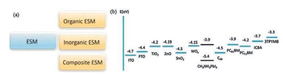
In a typical perovskite solar cells, electron selective contact material (ESM) is responsible for selective extraction of electrons at the anode contact, adopted from dye-sensitized solar cells and blocking holes from recombination with injected electrons [21]. Similar to its counterpart HSM, the ESM can be divided into inorganic ESM, organic ESM and composite ESM depending on the nature of the materials (Fig. 7a). The LUMO or conduction band energy levels of some ESMs used in PSCs are shown in Fig. 7b which are crucial to the performance of the device.

|
Download:
|
| Fig. 7. (a) Classification of electron selective hole-blocking materials; (b) Energy level diagram showing conduction band minimum/LUMO levels of various ETLs. Reproduced from Ref. [21] with permission from The Royal Society of Chemistry. | |
3. Electron selective hole-blocking materials (ESM) 3.1. Inorganic ESMs 3.1.1. TiO2
In a classic n-i-p device configuration, the most commonly used electron selective contact materials is compact TiO2 [67]. Some device configurations also include a thin mesoporous layer of TiO2, which is infiltrated and capped with the perovskite absorber. This type of device structure holds so far the highest reported PCE of a PSC [22]. The metal oxide scaffold is believed to provide an effective n-doping in this infiltrated layer, likely resulting in a favourable n-type/intrinsic homo junction within the perovskite layer [68]. It was supposed that the effective n-doping may be due to under-coordinated halides acting as shallow electron donors on the crystal surface, or due to a surface charge effect of the mesoporous metal oxide. Nazeeruddin group recently found by FIB-EDX analysis in a cross section of perovskite solar cell the nonuniform distribution of iodine element from mesoporous layer to capping layer [34].
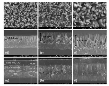
In general, the compact TiO2 blocking layer is deposited using a spin-coating technique or spray pyrolysis method. The deposition of mesoporous TiO2 scaffold is now dominated by spin-coating an organotitanium precursor, while doctor blade technique derived from the DSSCs is used in rare cases. Optimal infiltration of the perovskite and HSM into the pores of the mesoporous TiO2 is desirable for highly efficient devices. Kim et al. investigated the thickness dependence of device performance and they found that as the TiO2 thickness increases, the VOC and FF values decreases significantly [69]. Nazeeruddin group reported on a CH3NH3PbI3/ TiO2 heterojunction solar cell using anatase nanosheets with domain (001) facets as the ESM with a side length of 30 nm and a thickness of 7 nm [17]. The constructed device demonstrated a moderate performance with JSC of 16.1 mA/cm2, VOC of 0.631 V, FF of 0.57 corresponding to 5.5% efficiency. The lower performance is arguably due to the absence of HSM in the device structure. Later, collaborative work between Park and Grätzel demonstrated high performance perovskite solar cells based on 0.6 mm rutile TiO2 nanorods along with CH3NH3PbI3 perovskite nanodots (Fig. 8) [70]. The rutile nanorods were successfully hydrothermally grown and the lengths were controllable via the reaction time. They reported that shorter rutile nanorods were remarkably better for the infiltration of HSM compared to those of with longer length. The device produces 9.4% efficiency along with JSC of 15.6 mA/cm2, VOC of 0.955 V and FF of 0.63.

|
Download:
|
| Fig. 8. (a-c) Surface and (d-f) cross-sectional FESEM images of rutile TiO2 nanorods grown on FTO substrate. (g-i) Cross-sectional SEM images of solid state DSSCs based on perovskite CH3NH3PbI3-sensitized rutile TiO2 nanorod photoanode, the spiroMeOTAD hole transporting layer, and the Au cathode. Reprinted with permission from the American Chemical Society [70]. | |
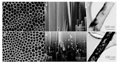
Gao et al. initiated a work on freestanding TiO2 nanotube array film prepared by means of two-step anodization process and detached from the substrate by in situ field-assisted chemical dissolution and later transferred onto FTO substrate which was covered by a TiO2 blocking layer (Fig. 9) [71]. As comparison, the control device with TiO2 nanoparticle (similar thickness) was also developed and they found that their proposed TiO2 nanotube has a better absorption than that with TiO2 nanoparticles most likely due to the improved light trapping capability (Fig. 9). Moreover, they also observed that TiO2 nanotube array presented a higher charge collection efficiency compared to those of TiO2 nanoparticles. Their perovskite solar cells constructed with TiO2 nanotube yielded 6.25% efficiency with a JSC of 17.9 mA/cm2. These observations show that the improvement of TiO2 nanotube perovskite solar cells was attributed to both the improved light harvesting and reduced carrier recombination.

|
Download:
|
| Fig. 9. Morphology characterization of TiO2 nanotubes before and after the perovskite dye deposition. (a-c) SEM images of the top view (a), the cross-section image (b) and the TEM image (c) of pristine TiO2; (d-f) SEM images of the top view (d), the cross-section image (e) and the TEM image (f) of TiO2 nanotubes with CH3NH3PbI3 deposition. Reprinted with permission from the Royal Society of Chemistry [71]. | |
Despite being widely used as ESM, TiO2 has some limitations which could possibly lead to Ohmic losses or non-ideal space charge distribution with perovskite solar cells. Pathak et al. suggested that Al doping reduces the number of sub-bandgap states of TiO2 (improving the VOC) and greatly improves electron conductivity [72]. Perovskite solar cells with 0.3 mol% Al-doping level produced 13.8% efficiency compared to those of without doping of only 11.13%. The significant improvement in solar cells with doped TiO2 was mainly due to the improved quantum efficiency leading to JSC of 20 mA/cm2. Prior to this study, Zhou et al. reported Yttrium doped TiO2 in the perovskite solar cells which led to 19.3% efficiency [73]. Doped TiO2 produced a better conductivity compared to undoped TiO2 film (2 × 10⁻⁵ S/cm vs. 6 × 10⁻⁶ S/cm) which was due to the improved carrier concentration as well as decreased series resistance in device. It is worth to note that the conductivity of doped TiO2 was similar to our frequently used HSM, spiro-OMeTAD and 10-order of magnitudes higher compared with undoped TiO2.
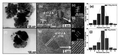
Nazeeruddin group also successfully investigated the use of Y3+-substituted TiO2 (0.5% Y-TiO2) in perovskite solar cells comprising CH3NH3PbI3 and spiro-OMeTAD (Fig. 10) [74]. The doped devices produced 11.2% efficiency and observed 15% enhancement in the JSC compared with pristine TiO2. The JSC improvement was arguably because the effect of Y3+ on the dimensions of perovskite nanoparticles formed on the semiconductor surface.

|
Download:
|
| Fig. 10. TEM analysis of 0.5%Y-TiO2/CH3NH3PbI3 and TiO2/CH3NH3PbI3 electrodes. (a-e) 0.5%Y-TiO2/CH3NH3PbI3 electrode and (f-j) TiO2/CH3NH3PbI3 electrode: (a and f) BFTEM micrographs; (b and g) HRTEM micrographs of dark colored (encircled) individual nanoparticles deposited on TiO2; (c and h) FFT patterns obtained from the corresponding HRTEM; (d and i) zoomed HRTEM showing prominent lattice fringes; (e and j) histograms showing particle size distribution. Reprinted with permission from The Royal Society of Chemistry [74]. | |
3.1.2. ZnO
Apart from TiO2, there have been a lot of reports employing ZnO as a potential replacement to TiO2 for PSCs due to its comparable energy levels and good transport properties (bulk mobility: 205-300 cm2/V/s). Kumar et al. were among the first to employ ZnO compact layer formed by electrodeposition technique and ZnO nanorods prepared by chemical bath deposition (Fig. 11) [75]. The blocking-ZnO/ZnO nanorods based perovskite solar cells documented 8.90% efficiency with astonishingly high JSC of 16.98 mA/cm2 compared to planar ZnO based device only 5.54% with a greatly lower JSC of 11.27 mA/cm2. In this study, they argued that the improved JSC was due to better charge generation and collection efficiency because of the enhanced light scattering and larger heterojunction interface.

|
Download:
|
| Fig. 11. FESEM images of (a) top view of the ZnO compact layer electrodeposited on FTO (inset shows high resolution image); (b) cross-sectional view of perovskite islands on the ZnO compact layer; (c) cross-sectional view of the complete planar ZnO device; FTO (blue), ZnO BL (red), perovskite + spiro (light green), gold (yellow); (d) top view of ZnO nanorods grown on the ZnO compact layer on the FTO substrate; (e) cross-sectional view of perovskite islands on ZnO nanorods; and (f) crosssectional view of the complete ZnO nanorod device; FTO (blue), ZnO BL (red), ZnO nanorod + perovskite (purple), spiro (green), gold (yellow). Reprinted with permission from the Royal Society of Chemistry [75]. | |
Park's group also reported on ZnO nanorods grown on the ZnO seed layer from solution to fabricate their CH3NH3PbI3 perovskite solar cells (Fig. 12) [76]. The lengths and diameters of ZnO nanorods were manipulated by precursor concentration as well as growth time. They were able to obtained 11.13% efficiency with JSC of 20.08 mA/cm2, VOC of 0.991 V and FF of 0.56. Their control devices with TiO2 nanorods demonstrated a slightly less performance with only 10.02% efficiency and they attributed the decrease in device performance because of a low VOC (0.869 V). The slightly lower VOC was due to the lower conduction band of TiO2 with respect to ZnO nanorods as well as slower recombination properties.

|
Download:
|
| Fig. 12. Surface SEM images of hexagonal ZnO nanorods grown at (a) 20, (b) 25, (c) 30, and (d) 35 mM of the precursor solution containing equimolar zinc nitrate hexahydrate and hexamethylenetetramine. The ZnO seed layer deposited FTO substrates were immersed in the precursor solution at 90 ℃ for 180 min. Insets represent distribution of diameters of ZnO nanorods. Reprinted with permission from the American Chemical Society [76]. | |
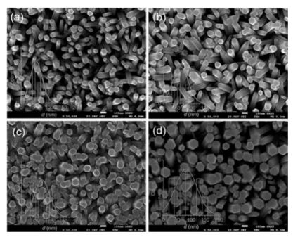
Liu and Kelly independently demonstrated a planar perovskite solar cells featuring ZnO nanoparticles [6]. They demonstrated the capability of ZnO nanoparticles under two different types of devices: rigid and flexible formats. A notable performance was demonstrated for rigid format with 15.7% efficiency while 10.2% efficiency was reported for flexible perovskite solar cells. The high performance of rigid solar cell was due to the unconstrained CH3NH3PbI3 perovskite crystallite growth that took place in the absence of a mesoporous scaffold. However, ZnO suffers from the issue of chemical unstability [77].
3.1.3. SnO2Recently, SnO2 has emerged as another promising ESM with a high transparency and electron mobility (bulk mobility: 240 cm2/ V/s). Li et al. successfully utilized TiCl4 treated SnO2 nanoparticle as ESM in PSCs and the efficiency of the device with SnO2 films exceeded 10% [78]. Song et al. demonstrated that low-temperature processed SnO2 compact layer based planar PSCs could achieve a high PCE of 13.0%, which is highly durable with exposure to the ambient air environment for 30 days [79]. Another low temperature sol-gel fabricated SnO2 ESM was reported by Yang et al. An average efficiency of 16.02% was obtained without hysteresis [80]. Recently, Correa Baena et al. used a 15 nm thick SnO2 as ESM processed by atomic layer deposition (ALD) technique [81]. They showed hysteresis-free, high stabilized planar perovskite solar cell with a high voltage of 1.19 V.
3.2. Organic ESMsIn contrast to the inorganic ESMs, a smaller variety of organic materials has been explored as an alternative electron-selective contact materials, of which: BCP, C60, ICBA, PCBM are a few examples (Fig. 13) [21]. These ESMs are normally used in a p-i-n structured PSC devices, where the perovskite are coated upon a ptype HSM (for example PEDOT:PSS or nickel oxide) before the deposition of an electron selective charge collection layer on top of the perovskite. It is worth mentioning that these so called inverted PSCs with all organic contacts generally exhibit little hysteresis. The use of fullerene (C60, 31) and its derivatives was proposed by Jeng et al. [82]. Their device consists of ITO/PEDOT:PSS/ CH3NH3PbI3/C60/BCP/Al. A thin bathocuproine (BCP, 30) film functioned as a hole-blocking layer and they obtained 3.0% efficiency. When substitute C60 with PCBM (33) and ICBA (32), the efficiency improved to 3.9% and 3.4%, respectively. The results suggest the existence of donor-acceptor interface at the CH3NH3PbI3/fullerene heterojunction as well as the variation of device performance by acceptors of various LUMO levels. Snaith and collaborators constructed perovskite/PCBM flexible solar cells with a conversion efficiency of 6% and later the performance was slightly improved to 7% by Bolink's group adopting similar device architecture [83].

|
Download:
|
| Fig. 13. Chemical structures of selected organic ESMs used in PSCs. | |
3.3. Composite ESM
In general, TiO2 surfaces possess deep mid-gap states which enable non-radiative recombination channels at the perovskite interface that will eventually influence the device performance [84]. Hence, voluminous reports have been put forward to passivate surface traps of TiO2 surface for example by introducing an polar molecules [85], C60-SAM [55, 86], graphene quantum-dots [87-90], antimony (Ⅲ) sulfide (Sb2S3) [91]. It was found that the introduction of low band gap antimony (Ⅲ) sulfide (Sb2S3) not only modified the TiO2/perovskite interface but also enhanced the lifetime of the device even under continuous light illumination. From this study, Ito and coworkers believe that the light degradation takes place at the TiO2/CH3NH3PbI3 interface. Another effective way of controlling the charge recombination is to introduce some wide band gap semiconductors at the TiO2 surface like PbI2 [34], MgO [92], Y2O3 and Al2O3 [93] passivation. For example, an ultrathin MgO nanolayer can be introduced to the interface between the TiO2 layer and perovskite layer. This modification could retard the electron/hole recombination at the TiO2/CH3NH3PbI3 interface, thus leading to the enhancement in both Voc and PCE.
4. Conclusions and outlooksNowadays, both n-i-p and p-i-n device structures are reported to give high performance PSCs with PCEs above 20%. In a p-i-n architecture, holes are extracted by the bottom electrode, transparent indium tin oxide (ITO) or FTO in most cases, while electrons are extracted at the bottom electrode in the n-i-p architectures. The efficiency of the device is determined by the charge selective contact materials. Hence, by introducing proper contact materials with good charge selectivity, one could potentially reduce interfacial charge recombination as well as increase device performance. In order to efficiently extract hole to the anode electrode, hole selective materials should possess a suitable energy alignment with perovskite film. It is of crucial importance that the conduction band (CB) or the lowest unoccupied molecular orbital (LUMO) of the HSM should be high enough to efficiently block the back diffusion of electrons to the cathode electrode. Identical principles also apply to the electron selective layers. It is desirable that selective contact materials to have larger bandgaps than that of perovskite film to avoid the excitons from recombining at the electrode. Also, it is crucial to design and synthesis selective contact materials with high conductivity to reduce the series resistance of the perovskite solar cell. In the past few years, copious selective contact materials have been proposed. It has been observed that both selective contacts contribute to enhance the cell FF, while the hole-selective contact is mainly responsible for the high VOC [94]. However, nowadays, most efficient HSMs need dopants to work properly, which decreases their ambient stability and degrade the perovskite layers. Therefore, it is necessary to develop more low-cost, dopantfree HSMs for stable PSCs. The dopant-free HTM can also protect the perovskite layer from exposure to moisture and UV light. On the other hand, the commonly used TiO2 ESM tend to generate radicals which is detrimental to the stability of perovskite film. Therefore, the development of non-photocatalytic ESM is also very important for the future commercialization of PSCs.
AcknowledgmentsY.M. YU acknowledges the National Natural Science Foundation of China (No. 21404045). P. [70_TD$DIFF][42_TD$DIFF]Gao acknowledges the financial support from "Hundred Talents Program" of the Haixi Institute Chinese Academy of Sciences (No. 1017001).
| [1] | W.S. Yang, J.H. Noh, N.J. Jeon, et al., . Science 348(2015)1234–1237. DOI:10.1126/science.aaa9272 |
| [2] | D. Bi, W. Tress, M.I. Dar, et al., . Sci. Adv. 2(2016)e1501170–e1501170. |
| [3] | P. Gao, M. Grätzel, M.K. Nazeeruddin. . Energy Environ. Sci. 7(2014)2448–2463. DOI:10.1039/C4EE00942H |
| [4] | J. Burschka, N. Pellet, S.J. Moon, et al., . Nature 499(2013)316–319. DOI:10.1038/nature12340 |
| [5] | M. Liu, M.B. Johnston, H.J. Snaith. . Nature 501(2013)395–398. DOI:10.1038/nature12509 |
| [6] | D. Liu, T.L. Kelly. . Nat. Photonics 8(2013)133–138. DOI:10.1038/nphoton.2013.342 |
| [7] | Z. Xiao, C. Bi, Y. Shao, et al., . Energy Environ. Sci. 7(2014)2619–2623. DOI:10.1039/C4EE01138D |
| [8] | H.S. Ko, J.W. Lee, N.G. Park. . J. Mater. Chem. A 3(2015)8808–8815. DOI:10.1039/C5TA00658A |
| [9] | N.J. Jeon, J.H. Noh, Y.C. Kim, et al., . Nat. Mater. 13(2014)897–903. DOI:10.1038/nmat4014 |
| [10] | P. Ganesan, K. Fu, P. Gao, et al., . Energy Environ. Sci. 8(2015)1986–1991. DOI:10.1039/C4EE03773A |
| [11] | H. Li, K. Fu, A. Hagfeldt, et al., . Angew. Chem. Int. Ed. 53(2014)4085–4088. DOI:10.1002/anie.201310877 |
| [12] | Q. Lin, A. Armin, R.C.R. Nagiri, P.L. Burn, P. Meredith. . Nat. Photonics 9(217)106–112. |
| [13] | S. Ye, W. Sun, Y. Li, et al., . Nano Lett. 15(2015)3723–3728. DOI:10.1021/acs.nanolett.5b00116 |
| [14] | X. Xu, Z. Liu, Z. Zuo, et al., . Nano Lett. 15(2015)2402–2408. DOI:10.1021/nl504701y |
| [15] | J.M. Ball, M.M. Lee, A. Hey, H.J. Snaith. . Energy Environ. Sci. 6(2013)1739. DOI:10.1039/c3ee40810h |
| [16] | D. Liu, J. Yang, T.L. Kelly. . J. Am. Chem. Soc. 136(2014)17116–17122. DOI:10.1021/ja508758k |
| [17] | L. Etgar, P. Gao, Z. Xue, et al., . J. Am. Chem. Soc. 134(2012)17396–17399. DOI:10.1021/ja307789s |
| [18] | M.A. Green. . Phys. E Low-Dimens. Syst. Nanostruct. 14(2002)11–17. DOI:10.1016/S1386-9477(02)00354-5 |
| [19] | Z. Yu, L. Sun. . Adv. Energy Mater. 5(2015)1500213. DOI:10.1002/aenm.201500213 |
| [20] | S. Ameen, M.A. Rub, S.A. Kosa, et al., . ChemSusChem 9(2016)10–27. DOI:10.1002/cssc.201501228 |
| [21] | G. Yang, H. Tao, P. Qin, W. Ke, G. Fang. . J. Mater. Chem. A 4(2016)3970–3990. DOI:10.1039/C5TA09011C |
| [22] | D. Bi, C. Yi, J. Luo, et al., . Nat. Energy 1(2016)16142. DOI:10.1038/nenergy.2016.142 |
| [23] | K. Rakstys, M. Saliba, P. Gao, et al., . Angew. Chem. Int. Ed. 55(2016)7464–7468. DOI:10.1002/anie.201602545 |
| [24] | K. Rakstys, S. Paek, M. Sohail, et al., . J. Mater. Chem. A 4(2016)18259–18264. DOI:10.1039/C6TA09028A |
| [25] | M. Saliba, S. Orlandi, T. Matsui. . Nat. Energy 1(2016)15017. DOI:10.1038/nenergy.2015.17 |
| [26] | D. Bi, B. Xu, P. Gao, et al., . Nano Energy 23(2016)138–144. DOI:10.1016/j.nanoen.2016.03.020 |
| [27] | A. Abate, S. Paek, F. Giordano, et al., . Energy Environ. Sci. 8(2015)2946–2953. DOI:10.1039/C5EE02014J |
| [28] | N.J. Jeon, J. Lee, J.H. Noh, et al., . J. Am. Chem. Soc. 135(2013)19087–19090. DOI:10.1021/ja410659k |
| [29] | P. Qin, S. Paek, M.I. Dar, et al., . J. Am. Chem. Soc. 136(2014)8516–8519. DOI:10.1021/ja503272q |
| [30] | K. Rakstys, A. Abate, M.I. Dar, et al., . J. Am. Chem. Soc. 137(2015)16172–16178. DOI:10.1021/jacs.5b11076 |
| [31] | S. Paek, I. Zimmermann, P. Gao, et al., . Chem. Sci. 7(2016)6068–6075. DOI:10.1039/C6SC01478J |
| [32] | S. Paek, M.A. Rub, H. Choi, et al., . Nanoscale 8(2016)6335–6340. DOI:10.1039/C5NR05697G |
| [33] | S. Kazim, F.J. Ramos, P. Gao, et al., . Energy Environ. Sci. 8(2015)1816–1823. DOI:10.1039/C5EE00599J |
| [34] | Y. Zhang, P. Gao, E. Oveisi, et al., . J. Am. Chem. Soc. 138(2016)14380–14387. DOI:10.1021/jacs.6b08347 |
| [35] | Y. Guo, C. Liu, K. Inoue, et al., . J. Mater. Chem. A 2(2014)13827–13830. DOI:10.1039/C4TA02976C |
| [36] | Z. Zhu, Y. Bai, H.K.H. Lee, et al., . Adv. Funct. Mater 24(2014)7357–7365. DOI:10.1002/adfm.v24.46 |
| [37] | P. Qin, N. Tetreault, M.I. Dar, et al., . Adv. Energy Mater. 5(2015)1400980. DOI:10.1002/aenm.201400980 |
| [38] | B. Cai, Y. Xing, Z. Yang, W.H. Zhang, J. Qiu. . Energy Environ. Sci. 6(2013)1480. DOI:10.1039/c3ee40343b |
| [39] | A. Dubey, N. Adhikari, S. Venkatesan, et al., . Sol. Energy Mater. Sol. Cells 145(2016)193–199. DOI:10.1016/j.solmat.2015.10.008 |
| [40] | Y.S. Kwon, J. Lim, H.J. Yun, Y.H. Kim, T. Park. . Energy Environ. Sci. 7(2014)1454. DOI:10.1039/c3ee44174a |
| [41] | J.H. Heo, S.H. Im, J.H. Noh, et al., . Nat. Photonics 7(2013)486–491. DOI:10.1038/nphoton.2013.80 |
| [42] | W. Nie, H. Tsai, R. Asadpour, et al., . Science 347(2015)522–525. DOI:10.1126/science.aaa0472 |
| [43] | J. Seo, N.J. Jeon, W.S. Yang, et al., . Adv. Energy Mater. 5(2015)1501320. DOI:10.1002/aenm.201501320 |
| [44] | F. Javier Ramos, M. Ince, M. Urbani, et al., . DaltonTrans 44(2015)10847–10851. DOI:10.1039/C5DT00396B |
| [45] | P. Gao, K.T. Cho, A. Abate, et al., . Phys. Chem. Chem. Phys. 18(2016)27083–27089. DOI:10.1039/C6CP03396B |
| [46] | H.H. Chou, Y.H. Chiang, M.H. Li, et al., . ACS Energy Lett (2016)956–962. |
| [47] | L. Calió, .Kazim S., M. S Grätzel. Ahmad, Angew. Chem. Int.Ed 55(2016)14522–14545. DOI:10.1002/anie.201601757 |
| [48] | J. Liu, Y. Wu, C. Qin, et al., . Energy Environ. Sci. 7(2014)2963. DOI:10.1039/C4EE01589D |
| [49] | Z. Li, Z. Zhu, C.C. Chueh, et al., . J. Am. Chem. Soc. 138(2016)11833–11839. DOI:10.1021/jacs.6b06291 |
| [50] | F. Zhang, C. Yi, P. Wei, et al., . Adv. Energy Mater. 6(2016)1600401. DOI:10.1002/aenm.201600401 |
| [51] | F. Zhang, X. Liu, C. Yi, et al., . ChemSusChem 9(2016)2578–2585. DOI:10.1002/cssc.201600905 |
| [52] | X. Zhao, F. Zhang, C. Yi, et al., . J. Mater. Chem. A 4(2016)16330–16334. DOI:10.1039/C6TA05254A |
| [53] | D. Bi, A. Mishra, P. Gao, et al., . ChemSusChem 9(2016)433–438. DOI:10.1002/cssc.201501510 |
| [54] | N.J. Jeon, J.H. Noh, W.S. Yang, et al., . Nature 517(2015)476–480. DOI:10.1038/nature14133 |
| [55] | A. Abrusci, S.D. Stranks, P. Docampo, et al., . Nano Lett. 13(2013)3124–3128. DOI:10.1021/nl401044q |
| [56] | S. Ryu, J.H. Noh, N.J. Jeon, et al., . Energy Environ. Sci. 7(2014)2614. DOI:10.1039/C4EE00762J |
| [57] | K.T. Cho, K. Rakstys, M. Cavazzini, et al., . Nano Energy 30(2016)853–857. DOI:10.1016/j.nanoen.2016.09.008 |
| [58] | C.V. Kumar, G. Sfyri, D. Raptis, E. Stathatos, P. Lianos. . RSC Adv. 5(2015)3786–3791. DOI:10.1039/C4RA14321C |
| [59] | F. Ghani, J. Kristen, H. Riegler. . J. Chem. Eng. Data 57(2012)439–449. DOI:10.1021/je2010215 |
| [60] | M. Li, Y. Li, S. Sasaki, et al., . ChemSusChem 9(2016)2862–2869. DOI:10.1002/cssc.201601069 |
| [61] | M. Xiao, M. Gao, F. Huang, et al., . ChemNanoMat 2(2016)182–188. DOI:10.1002/cnma.201500223 |
| [62] | J.A. Christians, R.C.M. Fung, P.V. Kamat. . J. Am. Chem. Soc 136(2014)758–764. DOI:10.1021/ja411014k |
| [63] | P. Qin, S. Tanaka, S. Ito, et al., . Nat. Commun. 5(2014)1–6. |
| [64] | Z. Zhu, Y. Bai, T. Zhang, et al., . Angew. Chem.-Int. Ed. 53(2014)12571–12575. |
| [65] | K.C. Wang, J.Y. Jeng, P.S. Shen, et al., . Sci. Rep. 4(2014)4756. |
| [66] | L. Hu, J. Peng, W. Wang, et al., . ACS Photonics 1(2014)547–553. DOI:10.1021/ph5000067 |
| [67] | N.G. Park, J. Phys. . Chem. Lett. 4(2013)2423–2429. |
| [68] | T. Leijtens, S.D. Stranks, G.E. Eperon, et al., . ACS Nano. 8(2014)7147–7155. DOI:10.1021/nn502115k |
| [69] | H.S. Kim, C.R. Lee, J.H. Im, et al., . Sci. Rep. 2(2012)591. |
| [70] | H.S. Kim, J.W. Lee, N. Yantara, et al., . Nano Lett. 13(2013)2412–2417. DOI:10.1021/nl400286w |
| [71] | X. Gao, J. Li, J. Baker, et al., . Chem. Commun. (Camb.) 50(2014)6368–6371. DOI:10.1039/C4CC01864H |
| [72] | S.K. Pathak, A. Abate, P. Ruckdeschel, et al., . Adv. Funct. Mater. 24(2014)6046–6055. DOI:10.1002/adfm.201401658 |
| [73] | H. Zhou, Q. Chen, G. Li, et al., . Science 345(2014)542–546. DOI:10.1126/science.1254050 |
| [74] | P. Qin, A.L. Domanski, A.K. Chandiran, et al., . Nanoscale 6(2014)1508–1514. DOI:10.1039/C3NR05884K |
| [75] | M.H. Kumar, N. Yantara, S. Dharani, et al., . Chem. Commun. 49(2013)11089–11091. DOI:10.1039/c3cc46534a |
| [76] | D.Y. Son, J.H. Im, H.S. Kim, N.G. Park. . J. Phys. Chem. C 118(2014)16567–16573. DOI:10.1021/jp412407j |
| [77] | X. Dong, H. Hu, B. Lin, J. Ding, N. Yuan. . Chem. Commun. 50(2014)14405–14408. DOI:10.1039/C4CC04685D |
| [78] | Y. Li, J. Zhu, Y. Huang, et al., . RSC Adv 5(2015)28424–28429. DOI:10.1039/C5RA01540E |
| [79] | J. Song, E. Zheng, J. Bian, et al., . J. Mater. Chem. A 3(2015)10837–10844. DOI:10.1039/C5TA01207D |
| [80] | W. Ke, G. Fang, Q. Liu, et al., . J. Am. Chem. Soc. 137(2015)6730–6733. DOI:10.1021/jacs.5b01994 |
| [81] | J. P. Correa Baena, L. Steier, W. Tress, et al., . Energy Environ. Sci 8(2015)2928–2934. DOI:10.1039/C5EE02608C |
| [82] | J.Y. Jeng, Y.F. Chiang, M.H. Lee, et al., . Adv. Mater. 25(2013)3727–3732. DOI:10.1002/adma.v25.27 |
| [83] | O. Malinkiewicz, A. Yella, Y.H. Lee, et al., . Nat. Photonics 8(2014)128–132. |
| [84] | I. Nakamura, N. Negishi, S. Kutsuna, et al., . J. Mol. Catal. A Chem. 161(2000)205–212. DOI:10.1016/S1381-1169(00)00362-9 |
| [85] | Y. Ogomi, A. Morita, S. Tsukamoto, et al., . J. Phys. Chem. C 118(2014)16651–16659. DOI:10.1021/jp412627n |
| [86] | K. Wojciechowski, S.D. Stranks, A. Abate, et al., . ACS Nano 8(2014)12701–12709. DOI:10.1021/nn505723h |
| [87] | Z. Zhu, J. Ma, Z. Wang, et al., . J. Am Chem. Soc. 136(2014)3760–3763. DOI:10.1021/ja4132246 |
| [88] | T. Liu, D. Kim, H. Han, et al., . Nanoscale 7(2015)10708–10718. DOI:10.1039/C5NR01433F |
| [89] | J.S. Yeo, R. Kang, S. Lee, et al., . Nano Energy 12(2015)96–104. DOI:10.1016/j.nanoen.2014.12.022 |
| [90] | C. Wang, Y. Tang, Y. Hu, et al., . RSC Adv. 5(2015)52041–52047. DOI:10.1039/C5RA09001F |
| [91] | S. Ito, S. Tanaka, K. Manabe, H. Nishino. . J. Phys. Chem. C 118(2014)16995–17000. DOI:10.1021/jp500449z |
| [92] | G.S. Han, H.S. Chung, B.J. Kim, et al., . J. Mater. Chem. A 3(2015)9160–9164. DOI:10.1039/C4TA03684K |
| [93] | Y. Ogomi, K. Kukihara, S. Qing, et al., . ChemPhysChem 15(2014)1062–1069. DOI:10.1002/cphc.201301153 |
| [94] | E.J. Juarez-Perez, M. F Wubler. Fabregat-Santiago. J. Phys. Chem. Lett 5(2014)680–685. |