 2017, Vol. 28


Perovskite solar cells (PVSCs) based on methylammonium (CH3NH3PbI3, denoted as MAPbI3) have been paid tremendous attentions as a promising next-generation solar cell technology due to the intense broadband absorption, high charge carrier mobility, low-cost precursor materials and simple solution processing of the perovskite films [1-6]. Recently, the power conversion efficiency (PCE) for the PVSCs has quickly increased to a certified value of 22.1% due to the development of composition engineering [7], interface engineering [8, 9] and processing methods [10]. However, most of the high efficiency PVSCs are usually fabricated in conventional mesoscopic architectures, which usually sandwich the perovskite layer between compact and mesoporous TiO2 layers and a hole-transporting layer (HTL) such as 2, 2, 7, 7-tetrakis (N, N-di-p-methoxyphenylamine)-9, 9-spirobifluorene (Spiro-OMeTAD) [11, 12]. These mesoscopic devices suffer from the issue of device processing due to the high sintering temperature for mesoporous and compact TiO2 layers. Thus there are growing interests in inverted planar heterojunction (PHJ) PVSCs with a simpler architecture of ITO/poly (3, 4-ethylenediox-ythiophene):polystyrenesulfonate (PEDOT:PSS)/MAPbI3/[6, 6]-phenyl-C61-butyric acid methyl ester (PC61BM)/cathode, because of the low temperature processing procedure and small hysteresis [13-15]. The PCEs over 18% have been achieved for this type of devices with small device areas [16, 17] and a certified PCE of 15% with large size (1 cm2) [18]. However, the widely used PEDOT:PSS is not an ideal HTL due to the insufficient electron-blocking capability and relatively low work function (-5.0 eV) which lead to low open-circuit voltage (VOC) (0.95-1.0 V). On the other hand, the hydrophilic and acidic nature of PEDOT:PSS is inferior to the device stability. Organic and inorganic materials with high work function and good chemical stability are tried to replace PEDOT:PSS [19, 20, 21]. For example, poly (bis (4-phenyl)(2, 4, 6-trimethylphenyl) amine) (PTAA) is one of the most efficient organic HTL which improves the VOC to 1.05-1.09 V from 0.92 V for PEDOT:PSS [22, 23]. The improvement is attributed to its high work function (-5.4 eV) which aligns well with the valance band (VB) of MAPbI3, forming ohmic contact at the HTL/MAPbI3 interface and thus reducing VOC loss. Also the hydrophobic surface of PTAA suppresses heterogeneous nucleation of perovskite, leading to large grain boundary and better crystallinity. In comparison with the organic transporting materials, transition metal oxides with high work function, such as MoO3 [24, 25], V2O5 [26], NiO [27] and WO3 [28], usually show high hole mobility, high optical transmittance, high chemical stability and low cost, which could be good candidates to replace PEDOT:PSS and have already been introduced into organic solar cells [29]. Among them, NiO [30], Mg-doped NiO (NixMg1-xO) [18], Cu-doped NiO [31], CuSCN [32], and CuS [33] were demonstrated as excellent hole-transporting materials for inverted planar PVSCs with PCEs of 14.42%, 18.4%, 15.4%, 16.0%, and 16.2% respectively. However, the processing of these materials is relatively complicate, for example, high temperature is needed for NiO and NixMg1-xO, which makes the device processing costly.
Copper oxides (CuOx), including cuprous oxide (Cu2O) and cupric oxide (CuO), are typical p-type semiconductors. Their advantages of earth-abundant source, low cost, and simplicity of preparation make them promising candidates for photovoltaic applications. In our previous work, we have successfully applied this material for organic solar cells as an efficient HTL, achieving a higher PCE and better stability than the ones using PEDOT:PSS as HTL [34]. Recently, copper oxides have also been employed as efficient HTL in PVSCs due to its proper energy levels that match those of MAPbI3 [35-38]. For instance, Hamid et al. have demonstrated the cuprous oxide by reactive magnetron sputtering as an efficient HTL and a PCE of 8.93% was achieved for conventional PHJ PVSCs [35]. Amlan et al. have prepared Cu2O through a successive ionic layer deposition and reaction (SILAR) method and the PCE for inverted PHJ PVSCs was 8.23% [36]. Wu et al. reported that the thermal oxidized ultrathin Cu2O film can serve as an efficient HTM, and a PCE of 11.'3% was obtained for inverted PHJ PVSCs [37]. However, the magnetron sputtering based method, SILAR method, and thermal oxidized method are complicated, costly and incompatible with the roll to roll techniques. Quite recently, Cu2O and CuO films prepared via in situ conversion of CuI film in aqueous NaOH solution were used as HTLs in inverted PHJ PVSCs with PCEs of 13.35% and 12.16%, respectively [38]. Even though these works validated the potential of using CuOx as efficient HTLs for PVSCs, facile and effective fabrication methods for CuOx film are still needed.
In this work, we demonstrated the facile solution-processed CuOx film can be applied to the inverted PHJ PVSCs with a PCE up to 17.43% as well as good stability. The CuOx film with high work function is simply spin-coated from a copper acetylacetonate precursor solution. Larger crystalline CH3NH3PbI3 domains are grown on the CuOx film. These results indicate that low-cost, simple-preparation and solution-processed CuOx is a promising HTM applicable in the high performance inverted PHJ perovskite solar cells.
2. Experimental 2.1. MaterialsUnless stated otherwise, all materials were purchased from Sigma-Aldrich and used as received. PC61BM was purchased from American Dyes Source, Inc. CH3NH3I (MAI) was purchased from Shanghai Materwin New Materials Co., Ltd. ZnO nanoparticles were synthesized by a sol-gel process using Zn acetate and tetramethylammonium hydroxide (TMAH), and dispersed in anhydrous ethanol with a concentration of 20 mg mL-1 [39].
2.2. Device fabrication and testingPrior to fabrication, the substrates were cleaned by sonication using detergent, deionized water, acetone, and isopropanol sequentially for every 15 min followed by 15 min of ultraviolet ozone (UV-ozone) treatment. PEDOT:PSS (Baytron P AI4083) was spin-coated on the ITO substrate to form a 35 nm film and baked at 140 ℃ for 2' min. The substrates were transferred to a glovebox. CuOx was fabricated by spin-coating a Cu (acac)2 chloroform solution with different concentrations (1, 2, 4, and 8 mg mL-1) on the ITO substrate and then annealed at 120 ℃ for 20 min in glovebox. Afterwards, the CuOx films were washed by methanol and followed by 15 min UV-Ozone treatment.
PbI2 (1 mol L-1) and DMSO (1 mol L-1) were dissolved in DMF under stirring at 70 ℃. The solution was kept at 70 ℃ during the whole procedure. The solution was then spin coated on the asprepared CuOx film at 6000 rpm for 60 s. Then a solution of MAI in 2-propanol (IPA) (50 mg mL-1) was dropped and spin-coated at 6000 rpm for 60 s. Afterwards, the as prepared films were heated at 90 ℃ for 15 min. After cooling down, a layer of [6, 6]-phenyl-C61-butyric acid methyl ester (PC61BM, 20 mg mL-1 in chlorobenzene) was spin-coated at 2000 rpm for 45 s. A hole-blocking layer was deposited via spin-coating ZnO nanoparticles in ethanol at 4000 rpm for 30 s on the top of PC61BM layer. Subsequently, samples were loaded into a vacuum deposition chamber (background pressure ≈5×10⁻⁴ Pa) todeposit a 100 nm thick Alcathode witha shadow mask defining an active device area of 5.5 mm2.
The J-V characteristics were measured with Keithley 2400 measurement source units with the devices maintained at room temperature in air. The photovoltaic response was measured under a calibrated solar simulator (Abet 300 W) at 100 mW cm-2, and the light intensity was calibrated with a standard photovoltaic reference cell. The EQE spectrum was measured using a Stanford Research System Model SR83' Lock-in Amplifier unit coupled with a monochromator and a 5'' W xenon lamp, and a calibrated Si photodiode with known spectral response was used as a reference.
2.3. Films characterizationThe X-ray diffraction (XRD) patterns were recorded at a scan rate of 5° min-1 on the Rigaku D/max-2550PC X-ray diffractometer with Cu Ka radiation (1.5406 nm). X-ray photoelectron spectroscopy (XPS) and ultraviolet photoelectron spectrum (UPS) measurements were conducted using an ESCALAB 250Xi (Thermo) system. The UV-visible absorption spectra were measured on a Varian CARY100 Bio spectrophotometer. The SEM data were scanned by S-4800 (Hitachi) field-emission scanning electron microscope (FESEM). Atom force microscopy (AFM) images were obtained using a Veeco Multimode atomic force microscopy in the tapping mode. The photoluminescence (PL) spectra (both of steady-state and transient spectra) are measured using an FluoroMax-4 HORIBA Jobin Yvon spectrofluorometer.
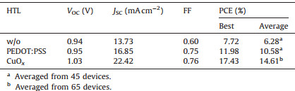
3. Results and discussion 3.1. CuOx film characterizationThe CuOx film is fabricated by simply spin-coating a copper acetylacetonate (Cu (acac)2) chloroform solution on ITO and annealed at 120 ℃ for 20 min with UV-Ozone treatment for 15 min, which is modified from our previous work [34]. The chemical component of the as-prepared film was confirmed by Xray photoelectron spectroscopy (XPS) with Cu2+/Cu+ ratio of about 3.2:1 (Fig. S1a in Supporting information). Such solution-processed CuOx thin film has a smooth surface with a RMS of 3.5 nm (Fig. S1b) and a high transparency similar to ITO in the visible range (Fig. S1c). The work function (WF) of CuOx film was measured by ultraviolet photoelectron spectrum (UPS). As shown in Fig. 1, the WFs of bare ITO and ITO/PEDOT:PSS are 4.4 eV and 5.0 eV, respectively, which are close to the reported values [40, 41]. ITO/CuOx however gives a higher WF of 5.4 eV, which aligns well with the valance band (VB) of MAPbI3 for ohmic contact [38]. These results indicate that CuOx could be potentially used as an excellent HTL in PVSCs.

|
Download:
|
| Figure 1. UPS spectra of the various HTLs on ITO and the bare ITO. | |
3.2. Perovskite film characterization
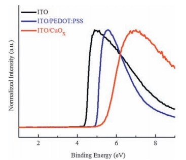
The film formation and surface morphology of the perovskite layer is heavily dependent on the substrates and is crucial in determining the performance of solar cells [42-44], and thus the morphology of the perovskite films on various HTLs of CuOx and PEDOT:PSS are characterized by scanning electron microscopy (SEM) (Fig. 2). The MAPbI3 films are fabricated via two-step coating method. All films are compact and pinhole-free, and the perovskite film on top of CuOx shows the largest grain domains and reduced grain boundaries. The film quality is further analyzed by X-ray diffraction (XRD), which is shown in Fig. 3a. Intense XRD signals are observed for the crystalline MAPbI3 films on all substrates. The diffraction intensity of MAPbI3 film on CuOx is slightly stronger than that of perovskite films on bare ITO and PEDOT:PSS. The intensity ratio for peaks at 14.5° on bare ITO, PEDOT:PSS, and CuOx is 1:1:1.2, indicating higher crystallinity for MAPbI3 film on CuOx. The higher crystallinity of MAPbI3 film on CuOx layer is also supported by its higher absorption as shown in Fig. 3b.

|
Download:
|
| Figure 2. Top view (a, b, c) and cross-sectional (d, e, f) SEM images of perovskite films fabricated on top of bare ITO (a, d), PEDOT:PSS (b, e), and CuOx (c, f). | |

|
Download:
|
| Figure 3. (a) XRD patterns of ITO/perovskite, ITO/PEDOT:PSS/perovskite and ITO/CuOx/perovskite on glass substrate. The star marked peaks belong to ITO. (b) UV-vis absorption and steady photoluminescence (PL) spectra of the optimized perovskite films on different HTLs. (c) Time-resolved PL measurements taken at the peak emission wavelength (765 nm) of the various HTLs. A 5 mW picosecond pulsed diode laser at 638.8 nm excited on the surface sided of films. | |
To investigate the hole-extraction ability of various HTLs, steady-state photoluminescence (PL) and time-resolved PL decay were conducted for MAPbI3 films on different substrates. As illustrated in Fig. 3b, various levels of PL quenching were observed and the stronger PL quenching was found for MAPbI3 on CuOx than on PEDOT:PSS, indicating the better hole-extraction ability of CuOx films. The time-resolved PL decays measured at the peak emission at 765 nm were shown in Fig. 3c. The MAPbI3 only film exhibits an averaged decay time (Ave. t) of 523 ns, while it decreased to 17' and 66 ns when it was applied on top of PEDOT:PSS and CuOx, respectively. This indicates the improved hole extraction and the charge dissociation were achieved at the CuOx/MAPbI3 interface. These results demonstrate that CuOx can be used as HTL replacing PEDOT:PSS for high performance PVSCs.
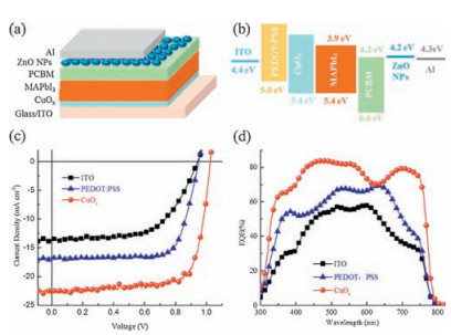
3.3. Photovoltaic performance of perovskite solar cellsAccording to the above results, we fabricated the inverted PHJ PVSCs in the structure of ITO/HTL/MAPbI3/PC61BM/ZnO/Al without and with different HTLs of CuOx and PEDOT:PSS (Fig. 4a). The energy level diagram of the device with different HTLs is shown in Fig. 4b. The devices with CuOx as HTL were optimized by adjusting the concentration of the CuOx precursor. As shown in Table 1, the best devices were obtained with the concentration of 2 mg mL-1. The current density-voltage (J-V) characteristics of the best devices with different HTLs measured under AM 1.5G conditions (100 mW cm-2) are presented in Fig. 4c and the relevant parameters are summarized in Table 2.

|
Download:
|
| Figure 4. Schematic of the device structure (a) and the energy-level diagram of the corresponding device (b). J-V curves (c) and EQE spectra (d) of the PVSCs without or with different HTLs. | |
|
|
Table 1 Device parameters of PVSCs fabricated from CuOx precursors with different concentrations. |

|
|
Table 2 Summarized solar cell parameters without and with different HTLs. |
As expected, PVSCs without HTL show poor performance with low VOC,JSC and FF. After incorporating a layer of PEDOT:PSS as HTL, the JSC increases from 13.73 mA cm-2 to 16.85 mA cm-2, FF increases from 0.60 to 0.75, VOC increases slightly from 0.94 V to 0.95 V, and the PCE significantly improved to 11.98% from 7.72%. However, it is still low comparing to the state-of-art PVSCs. The reason is mainly due to the low VOC and JSC resulted from the low work function and the inability to block electrons efficiently of PEDOT:PSS, as well as the small crystalline grains of MAPbI3 film on PEDOT:PSS. When CuOx is used as alternative, the best PCE surges to 17.43% which substantially surpass the performance of PEDOT:PSS based device, with significantly enhanced JSC of 22.42 mA cm2 and VOC of 1.03 V. FF is slightly increased to 0.76 comparing to the one based on PEDOT:PSS. The enhanced JSC can be interpreted as a consequence of the better charge-extraction ability of CuOx and larger grain domains, reduced grain boundaries of the MAPbI3 films. The higher VOC is resulted from the higher WF of CuOx which renders the ohmic contact at the CuOx/MAPbI3 interface and thus reducing VOC loss. On the other hand, reduced charge recombination originating from the larger grain domains of MAPbI3 film with reduced grain boundaries also attributes to the enhanced VOC. The external quantum efficiency (EQE) spectra of PVSCs without and with different HTLs are shown in Fig. 4d. Using CuOx as a HTL significantly improves the photocurrent in the region from 350 to 800 nm, which agrees well with the enhanced JSC. In summary, the performance enhancement of the CuOx-based device is attributed to the larger grain size, reduced recombination and more effective charge extraction described above.
The device hysteresis behavior and stabilized power output of the best device are provided in Fig. 5a and b, respectively. We can see that no apparent hysteresis is detected with forward and reverse scans. The photocurrent density and PCE as a function of time at the maximum power point (0.86 V) were performed to further confirm the accuracy of our PCE. As shown in Fig. 5b, both the photocurrent and PCE remain stable within 300 s, and a stable PCE over 15% is demonstrated. Fig. 5c shows the statistic histogram of device parameters. The device performance of PVSC with CuOx as HTL ranges from 12.80% to 17.43%, with the averaged value of 14.61%. In comparison, with PEDOT:PSS as HTL, a range from 8.51% to 11.98% and a much lower averaged PCE of 10.58%were obtained. In spite of the high photovoltaic efficiency, the long-term stability of PVSCs is of vital importance for practical applications. We therefore monitored the stabilities of different types of devices with various HTLs. Devices were tested without encapsulation in an ambient environment at 20 ℃ and with 20%-30% humidity. As shown in Fig. 5c, the PCEs of the CuOx-based devices maintain 90% of its initial efficiency after 650 h, while the PEDOT:PSS-based devices degrade to about 70% of the initial PCE. The degradation is mainly resulted from the reduced FF (Fig. S2 in Supporting information). These results indicate that CuOx is a promising holeextraction material for highly efficient PVSCs with good stability.

|
Download:
|
| Figure 5. (a) J-V curves of the best PVSCs measured by forward and reverse scans, fabricated using CuOx as HTL. (b) Stabilized photocurrent measurement of the best CuOx based PVSCs under 1 sun illumination. (c) Efficiency histograms of 65 PVSCs with CuOx as HTL and 45 PVSCs with PEDOT:PSS as HTL. (d) Normalized PCE as a function of storage time in air. | |
4. Conclusion
In conclusion, solution-processed CuOx films with high optical transmittance, high work function, proper surface properties and excellent hole-extraction ability are fabricated at low temperature and applied to PHJ PVSCs as efficient HTL. The high work function of the CuOx renders the ohmic contact at the MAPbI3/CuOx interface, reducing VOC loss. While compact and pinhole-free perovskite films with large grain domains are formed due to the proper surface properties, leading to the reduced carrier recombination and thus obtaining high JSC and VOC. Combining the excellent hole-extraction ability of the CuOx, high performance PHJ PVSCs with PCE up to 17.43% were demonstrated which is much higher than the ones of 11.98% based on PEDOT:PSS. The CuOxbased devices also show good stability in an ambient environment at room temperature with low humidity. Our work reveals the promising applicability of low-cost solution-processed CuOx in invert PHJ PVSCs with high performance and good stability.
AcknowledgmentsZ.-K. Yu and W.-F. Fu contributed equally to this work. This work was supported by the Major State Basic Research Development Program (No. 2014CB643503) and the National Science Foundation for Post-doctoral Scientists of China (No. 2015M580512). It is also partly supported by the program for Innovative Research Team in University of Ministry of Education of China (No. IRT13R54).
Appendix A. Supplementary dataSupplementary data associated with this article can be found, in the online version, at http://dx.doi.org/10.1016/j.cclet.2016.06.021.
| [1] | S.D. Stranks, G.E. Eperon, G. Grancini, Electron-hole diffusion lengths exceeding 1 micrometer in an organometal trihalide perovskite absorber. Science 342 (2013) 341–344. DOI:10.1126/science.1243982 |
| [2] | Q.Q. Lin, A. Armin, R.C.R. Nagiri, P.L. Burn, P. Meredith, Electro-optics of perovskite solar cells. Nat. Photon. 9 (2015) 106–112. |
| [3] | M.M. Lee, J. Teuscher, T. Miyasaka, T.N. Murakami, H.J. Snaith, Efficient hybrid solar cells based on meso-superstructured organometal halide perovskites. Science 338 (2012) 643–647. DOI:10.1126/science.1228604 |
| [4] | T.H. Liu, K. Chen, Q. Hu, Fast-growing procedure for perovskite films in planar heterojunction perovskite solar cells. Chin. Chem. Lett. 26 (2015) 1518–1521. DOI:10.1016/j.cclet.2015.09.022 |
| [5] | Z.S. Yang, L.G. Yang, G. Wu, M. Wang, H.Z. Chen, A heterojunction based on wellordered organic-inorganic hybrid perovskite and its photovoltaic performance. Acta Chim. Sin. 69 (2011) 627–632. |
| [6] | G. Wu, X.Q. Zhang, Z.W. Gu, H.Z. Chen, Progress of the research on organicInorganic hybrid perovskites based solar cells. Mater. China 34 (2015) 136–143. |
| [7] | N.J. Jeon, J.H. Noh, W.S. Yang, Compositional engineering of perovskite materials for high-performance solar cells. Nature 517 (2015) 476–480. DOI:10.1038/nature14133 |
| [8] | H.P. Zhou, Q. Chen, G. Li, Interface engineering of highly efficient perovskite solar cells. Science 345 (2014) 542–546. DOI:10.1126/science.1254050 |
| [9] | Q.F. Xue, C. Sun, Z.C. Hu, Recent advances in perovskite solar cells:morphology control and interfacial engineering. Acta Chim. Sin. 73 (2015) 179–192. DOI:10.6023/A14090674 |
| [10] | W.Y. Nie, H. Tsai, R. Asadpour, High-efficiency solution-processed perovskite solar cells with millimeter-scale grains. Science 347 (2015) 522–525. DOI:10.1126/science.aaa0472 |
| [11] | P. Qin, S. Tanaka, S. Ito, Inorganic hole conductor-based lead halide perovskite solar cells with 12.4% conversion efficiency. Nat. Commun. 5 (2014) 3834. |
| [12] | L. Wang, W.F. Fu, Z.W. Gu, Low temperature solution processed planar heterojunction perovskite solar cells with a CdSe nanocrystal as an electron transport/extraction layer. J. Mater. Chem. C 2 (2014) 9087–9090. DOI:10.1039/C4TC01875C |
| [13] | Y.C. Shao, Z.G. Xiao, C. Bi, Origin and elimination of photocurrent hysteresis by fullerene passivation in CH3NH3PbI3 planar heterojunction solar cells. Nat. Commun. 5 (2014) 5784. DOI:10.1038/ncomms6784 |
| [14] | P.W. Liang, C.Y. Liao, C.C. Chueh, Additive enhanced crystallization of solution-processed perovskite for highly efficient planar-heterojunction solar cells. Adv. Mater. 26 (2014) 3748–3754. DOI:10.1002/adma.v26.22 |
| [15] | J.H. Heo, D.H. Song, H.J. Han, Planar CH3NH3PbI3 perovskite solar cells with constant 17.2% average power conversion efficiency irrespective of the scan rate. Adv. Mater. 27 (2015) 3424–3430. DOI:10.1002/adma.v27.22 |
| [16] | C.G. Wu, C.H. Chiang, Z.L. Tseng, High efficiency stable inverted perovskite solar cells without current hysteresis. Energy Environ. Sci. 8 (2015) 2725–2733. DOI:10.1039/C5EE00645G |
| [17] | J.H. Heo, H.J. Han, D. Kim, T.K. Ahn, S.H. Im, Hysteresis-less inverted CH3NH3PbI3 planar perovskite hybrid solar cells with 18.1% power conversion efficiency. Energy Environ. Sci. 8 (2015) 1602–1608. DOI:10.1039/C5EE00120J |
| [18] | W. Chen, Y.Z. Wu, Y.F. Yue, Efficient and stable large-area perovskite solar cells with inorganic charge extraction layers. Science 350 (2015) 944–948. DOI:10.1126/science.aad1015 |
| [19] | C.Y. Huang, W.F. Fu, C.Z. Li, Dopant-free hole-transporting material with a C3h symmetrical truxene core for highly efficient perovskite solar cells. J. Am. Chem. Soc. 138 (2016) 2528–2531. DOI:10.1021/jacs.6b00039 |
| [20] | A. Krishna, D. Sabba, H.R. Li, Novel hole transporting materials based on triptycene core for high efficiency mesoscopic perovskite solar cells. Chem. Sci. 5 (2014) 2702–2709. DOI:10.1039/C4SC00814F |
| [21] | Y. Hua, B. Xu, P. Liu, High conductivity Ag-based metal organic complexes as dopant-free hole-transport materials for perovskite solar cells with high fill factors. Chem. Sci. 7 (2016) 2633–2638. DOI:10.1039/C5SC03569D |
| [22] | C. Bi, Q. Wang, Y.C. Shao, Non-wetting surface-driven high-aspect-ratio crystalline grain growth for efficient hybrid perovskite solar cells. Nat. Commun. 6 (2015) 7747. DOI:10.1038/ncomms8747 |
| [23] | Q. Wang, C. Bi, J.S. Huang, Doped hole transport layer for efficiency enhancement in planar heterojunction organolead trihalide perovskite solar cells. Nano Energy 15 (2015) 275–280. DOI:10.1016/j.nanoen.2015.04.029 |
| [24] | Z.A. Tan, D.P. Qian, W.Q. Zhang, Efficient and stable polymer solar cells with solution-processed molybdenum oxide interfacial layer. J. Mater. Chem. A 1 (2013) 657–664. DOI:10.1039/C2TA00325B |
| [25] | W.M. Qiu, A. Hadipour, R. Müller, Ultrathin ammonium heptamolybdate films as efficient room-temperature hole transport layers for organic solar cells. ACS Appl. Mater. Interfaces 6 (2014) 16335–16343. DOI:10.1021/am504606u |
| [26] | Z.A. Tan, W.Q. Zhang, C.H. Cui, Solution-processed vanadium oxide as a hole collection layer on an ITO electrode for high-performance polymer solar cells. Phys. Chem. Chem. Phys. 14 (2012) 14589–14595. DOI:10.1039/c2cp43125d |
| [27] | K.X. Steirer, P.F. Ndione, N.E. Widjonarko, Enhanced efficiency in plastic solar cells via energy matched solution processed NiOx interlayers. Adv. Energy Mater. 1 (2011) 813–820. DOI:10.1002/aenm.v1.5 |
| [28] | Z.A. Tan, L.J. Li, C.H. Cui, Solution-processed tungsten oxide as an effective anode buffer layer for high-performance polymer solar cells. J. Phys. Chem. C 116 (2012) 18626–18632. DOI:10.1021/jp304878u |
| [29] | F.Z. Wang, Z.A. Tan, Y.F. Li, Solution-processable metal oxides/chelates as electrode buffer layers for efficient and stable polymer solar cells. Energy Environ. Sci. 8 (2015) 1059–1091. DOI:10.1039/C4EE03802A |
| [30] | X.T. Yin, M.D. Que, Y.L. Xing, W.X. Que, High efficiency hysteresis-less inverted planar heterojunction perovskite solar cells with a solution-derived NiOx hole contact layer. J. Mater. Chem. A 3 (2015) 24495–24503. DOI:10.1039/C5TA08193A |
| [31] | J.H. Kim, P.W. Liang, S.T. Williams, High-performance and environmentally stable planar heterojunction perovskite solar cells based on a solutionprocessed copper-doped nickel oxide hole-transporting layer. Adv. Mater. 27 (2015) 695–701. DOI:10.1002/adma.201404189 |
| [32] | J.W. Jung, C.C. Chueh, A.K.Y. Jen, High-performance semitransparent perovskite solar cells with 10% power conversion efficiency and 25% average visible transmittance based on transparent CuSCN as the hole-transporting material. Adv. Energy Mater. 5 (2015) 1500486. DOI:10.1002/aenm.201500486 |
| [33] | H.X. Rao, W.H. Sun, S.Y. Ye, Solution-processed CuS NPs as an inorganic holeselective contact material for inverted planar perovskite solar cells. ACS Appl. Mater. Interfaces 8 (2016) 7800–7805. DOI:10.1021/acsami.5b12776 |
| [34] | Z.K. Yu, W.Q. Liu, W.F. Fu, An aqueous solution-processed CuOx film as an anode buffer layer for efficient and stable organic solar cells. J. Mater. Chem. A 4 (2016) 5130–5136. DOI:10.1039/C6TA00909C |
| [35] | B.A. Nejand, V. Ahmadi, S. Gharibzadeh, H.R. Shahverdi, Cuprous oxide as a potential low-cost hole-transport material for stable perovskite solar cells. ChemSusChem 9 (2016) 302–313. DOI:10.1002/cssc.201501273 |
| [36] | S. Chatterjee, A.J. Pal, Introducing Cu2O thin films as a hole-transport layer in efficient planar perovskite solar cell structures. J. Phys. Chem. C 120 (2016) 1428–1437. DOI:10.1021/acs.jpcc.5b11540 |
| [37] | W.L. Yu, F. Li, H. Wang, Ultrathin Cu2O as an efficient inorganic hole transporting material for perovskite solar cells. Nanoscale 8 (2016) 6173–6179. DOI:10.1039/C5NR07758C |
| [38] | C.T. Zuo, L.M. Ding, Solution-processed Cu2O and CuO as hole transport materials for efficient perovskite solar cells. Small 11 (2015) 5528–5532. DOI:10.1002/smll.v11.41 |
| [39] | L. Qian, J.H. Yang, R.J. Zhou, Hybrid polymer-CdSe solar cells with a ZnO nanoparticle buffer layer for improved efficiency and lifetime. J. Mater. Chem. 21 (2011) 3814–3817. DOI:10.1039/c0jm03799k |
| [40] | W.Y. Chen, L.L. Deng, S.M. Dai, Low-costsolution-processed copper iodide as an alternative to PEDOT:PSS hole transport layer for efficient and stable inverted planar heterojunction perovskite solar cells. J. Mater. Chem. A 3 (2015) 19353–19359. DOI:10.1039/C5TA05286F |
| [41] | T. Liu, L.J. Zuo, T. Ye, Low temperature processed ITO-free perovskite solar cells without a hole transport layer. RSC Adv. 5 (2015) 94752–94758. DOI:10.1039/C5RA20125J |
| [42] | L.J. Zuo, Z.W. Gu, T. Ye, Enhanced photovoltaic performance of CH3NH3PbI3 perovskite solar cells through interfacial engineering using self-assembling monolayer. J. Am. Chem. Soc. 137 (2015) 2674–2679. DOI:10.1021/ja512518r |
| [43] | Z.W. Gu, L.J. Zuo, T.T. Larsen-Olsen, Interfacial engineering of self-assembled monolayer modified semi-roll-to-roll planar heterojunction perovskite solar cells on flexible substrates. J. Mater. Chem. A 3 (2015) 24254–24260. DOI:10.1039/C5TA07008B |
| [44] | Z.P. Shao, X. Pan, X.H. Zhang, Influence of structure and morphology of perovskite films on the performance of perovskite solar cells. Acta Chim. Sin. 73 (2015) 267–271. DOI:10.6023/A14100721 |