 2016, Vol. 27


b Department of Applied Physics and Materials Research Centre, The Hong Kong Polytechnic University, Hong Kong, China ;
c Department of Mechanical Engineering, The University of Hong Kong, Hong Kong, China
Organic field-effect transistors (OFETs) have attracted tremendous interest for their low-cost,flexible and large-area electronic applications [1, 2]. Nowadays great achievements have been obtained in organic hole transporting semiconductors. Experimentally,the π-channel organic semiconductors have exhibited remarkable hole mobility approaching 100 cm2 V-1 s-1 [3-15]. In sharp contrast,development of the n-channel organic semiconductors is much slower. Up to now,electron mobility closeto 10 cm2 V-1 s-1 isonlydocumented inverylimited reports [16-25]. The uneven development in π-channel and n-channel organic semiconductors spurs investigations on the strategies to improve the n-channel materials because hole and electron transports are equally important for complementary circuits and other double-carrier devices [26-28].
The well-known reasons for the low mobility in the n-channel OFETs have close relations with high electron injection barriers [29, 30],electron traps [31-33] and dipolar disorder [34-36]. Accordingly,efforts have been made to avoid the negative effects of these factors on the performance of n-channel OFETs [37-39]. In addition to the n-channel OFETs,"unexpected" n-channel behavior has been occasionally found in typical π-channel OFETs [40-43]. For example,in 2005,Singh et al. found the significant electron
transport in pentacene on poly(vinyl alcohol) organic gate dielectric with Au as the source-drain electrodes,and the electron mobility up to 0.2 cm2 V-1 s-1 was obtained [41, 42]. Lately,Xu et al. reported that as a small amount (~14 mol%) of a typical n- channel molecule was added into a typical π-channel molecule,electron transport was observed [43]. Interestingly,the two molecules formed solid solutions instead of either phase separated blends [44, 45] and bi-layers [46-48] or co-crystals [49]. Further examination of these unusual device performances should provide implications for understanding and enhancing the electron transport in organic semiconductors. Very recently,we have found [50] a similar unusual electron transport in solution-grown single crystals of 6,13-bis(triisopropyl-silylethynyl) pentacene (TIPS-pentacene) [51]. Interestingly,although TIPS-pentacene is recognized as a typical π-channel semiconductor as Au is used for the source-drain electrodes [9, 52-56],electron transport emerges as TIPS-pentacene crystallizes on divinyl-tetramethyldisiloxane- bis(benzocyclobutene) (BCB) dielectric from non-polar solvents but does not in the case of polar solvents. In this work,we aim to reconfirm and further examine this unusual electron transport. Considering that gate dielectrics [33, 36, 57-60] and polar solvents have been shown to affect the electron transport dramatically,we investigate the effects of varied gate dielectrics and polar impurities on the electron transport in TIPS-pentacene single crystals.
2. ExperimentalCrystal growth and characterization: Poly(methyl methacrylate) (PMMA,Aldrich,Mw = 120kD),polystyrene (PS,Aldrich,Mw = 280 kD),poly(4-vinyl phenol) (PVP,Aldrich,Mw = 25 kD),poly(vinyl alcohol) (PVA,Aldrich,Mw= 130 kD) and poly(vinyli- dene fluoride-trifluoroethylene-chlorofluoroethylene) (P(VDF- TrFE-CFE)) were used as polymer dielectrics. P(VDF-TrFE-CFE) was synthesized according to the literature procedure [61, 62]. PMMA (1,5 mg/mL),PS (1 mg/mL) and PVP (1 mg/mL) were dissolved in n-butyl acetate,PVA (1,10 mg/mL) was dissolved in deionized water,and P(VDF-TrFE-CFE) (3 mg/mL) was dissolved in butanone,then the solutions were spin-coated onto highly doped silicon substrates with 300 nm SiO2. After dielectric layers coating,they were baked at 80 ℃ for about 2 h,except that the P(VDF-TrFE- CFE) and PVA (1,10 mg/mL) dielectrics were baked at 60 ℃ for 3 h and 24 h,respectively. The thicknesses of polymer dielectrics are around 2 nm (1 mg/mL),6 nm (3 mg/mL),10 nm (5 mg/mL) and 40 nm (10 mg/mL). TIPS-pentacene (Sigma-Aldrich) crystals were grown in ambient condition using the droplet-pinned crystallization (DPC) method onto the polymer dielectric covered highly doped silicon substrates with 300 nm SiO2. A TIPS- pentacene solution (15 mL,0.4mg/mL) dissolved in hexane (TCI,HPLC) was dropped onto a silicon substrate (1 cm × 1 cm) with a smaller piece of silicon wafer (0.3 cm × 0.3 cm,pinner) to pin the solution droplet. The silicon substrate was placed on a Teflon slide inside a Petri-dish (35 mm × 10 mm),allowing the solvent to slowly evaporate on a hotplate of 25 ± 1 ℃. Solution dried within three minutes and aligned crystals formed. For the treatment of polar solvent vapor,dichloromethane (CH2Cl2) (Aladdin,HPLC),chloroform (CHCl3) (Labor,HPLC),tetrahydrofuran (THF) (Aladdin,HPLC) and 1,2-dichloroethane (1,2-DCE) (Aladdin,HPLC) were used to treat the TIPS-pentacene single crystals grown on PMMA dielectric,as shown in Fig. 7a. For heat treatment,vapor-treated FETs were heated at 80 ℃ for 2 h and then cooled down naturally. The morphology of the crystals was characterized by optical microscopy (OM,Nikon LV100 POL) and Atomic force microscopy (AFM,Veeco 3D).

|
Download:
|
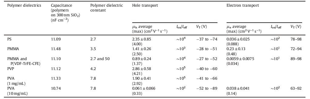
| Figure 1. (a) Molecular structures of the PS,PMMA,PVP,PVA and P(VDF-TrFE-CFE). (b) A schematic representation of the FET configuration,where S is the source,D is the drain and G is the gate. | |

|
Download:
|
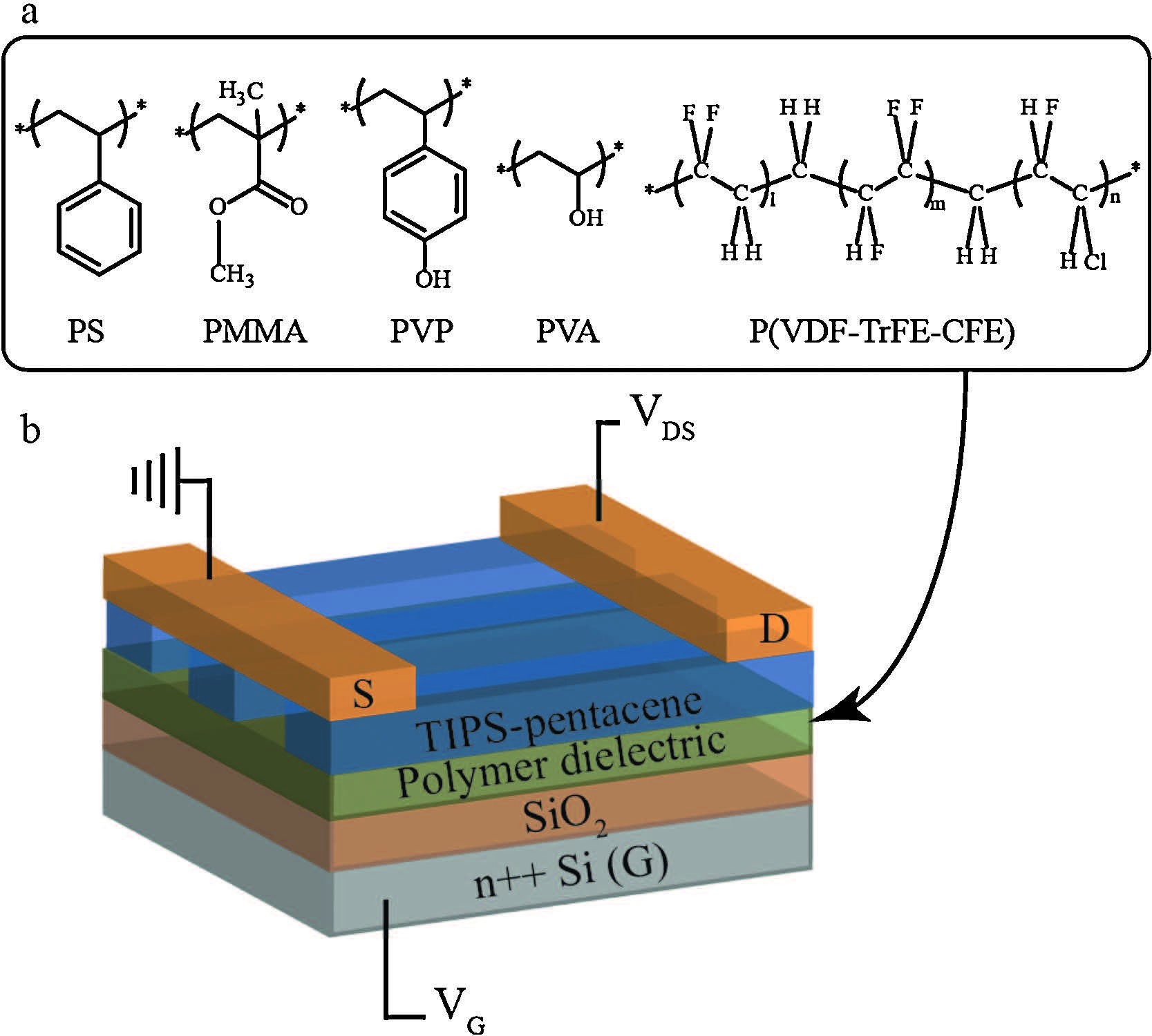
| Figure 2. Morphology of TIPS-pentacene single crystals grown on PMMA (a,f,k,p),PS (b,g,l,q),PMMA&PDVF-TrFE-CFE (c,h,m,r),PVP (d,i,n,s) and PVA (1 mg/mL) (e,j,o,t). (a-e) Optical microscopy (OM) images of the crystals. (f-j) OM images of the crystals under crossed-polarizers. (k-o) AFM images of surface morphology of crystals. (π-t) AFM images of surface steps on crystals. | |
FETs fabrication and measurement: FETs were constructed in a toπ-contact,bottom-gate configuration by depositing source and drain electrodes (90 nm Au),using a shadow mask with channel length (L) of 50 mm and width (W) of 1 mm. The real W/L value was measured (Fig. 3b inset) to calculate the mobility values. The devices were characterized in a N2 glovebox using a Keithley 4200- SCS semiconductor parameter analyzer. The capacitance was measured by Keysight E4980AL Precision LCR Meter and the values are listed in Table 1. For statistics,data of charge mobility are presented as mean ± SD.

|
Download:
|
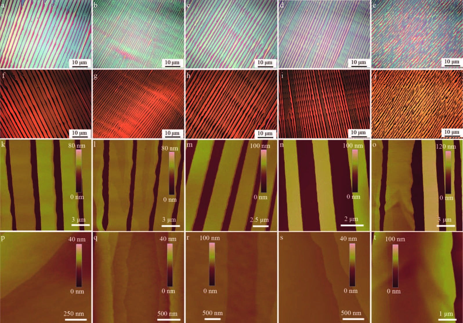
| Figure 3. FET characteristics of crystals grown on PMMA (a-d),PS (e-h) and PMMA&P(VDF-TrFE-CFE) (i-l). Typical transfer (a,b,e,f,i,j) and output (c,d,g,h,k,l) characteristics of the FETs in operation modes of π-channel (a,c,e,g,i,k) and n-channel (b,d,f,h,j,l) have been shown as well. Inset image in b: An OM image showing the method of W/L measurement. L was measured from the real channel length and W was measured from the contacting area of the crystals that cross the S and D electrodes. W was calculated by the equation: W = S(W1 + W2)/2. | |
|
|
Table 1 FET parameters of the TIPS-pentacene OFETs on various polymer dielectric layers coated on 300 nm SiO2. |
3. Results and discussion 3.1. The effect of gate dielectrics on electron transport
Five polymer dielectrics with different dielectric constants,PS (k 〜2.6),PMMA (k 〜3.5),(PVP) (k 〜4.2),(PVA) (k 〜7.8) and (P(VDF-TrFE-CFE) (k 〜50) [62],were selected to study their influence on the electron transport in TIPS-pentacene single crystals. Instead of pure polymer dielectrics,bilayer dielectrics with polymer films on 300 nm SiO2 were used for FETs,with the thick SiO2 layers to diminish the leakage currents and to maintain similar capacitance values. The molecular structures of the polymers and the polymer films surface morphology have been shown in Figs. 1a and S1 in Supporting Information,respectively. Hexane,a nonpolar solvent,was selected to grow the crystals in order to exclude the adverse effect of polar solvents on electron transport [24, 50]. TIPS-pentacene single crystals were grown using droplet-pinned crystallization (DPC) method [16, 63-65] directly on polymer dielectrics. Well-aligned single crystals were obtained (Figs. 2 and S2 in Supporting information). For the ribbons grown on PMMA,PS,PVP and PVA,the same color of individual ribbons under crossed-polarizers indicates their single-crystallinity (Fig. 2f-j). For those grown on P(VDF-TrFE-CFE),poor morphology of crystals was obtained due to the poor wettability of the solvent on the fluorinated surface (Fig. S2e-h in Supporting information). In order to avoid the negative effect of the poor morphology on the electron transport,a PMMA film around 10 nm thick,was covered onto the P(VDF-TrFE-CFE) surface through spin-coating to prepare a PMMA&P(VDF-TrFE-CFE) surface. As a result,the morphology of crystals grown on the PMMA&P(VDF-TrFE-CFE) was greatly improved and smooth single-crystalline ribbons were obtained (Fig. 2c,h,m,r).
Based on these aligned ribbon crystals,we proceeded to fabricate FETs by depositing Au source and drain electrodes through a shadow mask in a toπ-contact,bottom-gate configuration (Fig. 1b). Since the crystals did not fully cover the channel,the active W/L value was measured to calculate the mobility (Fig. 3b,inset). All the devices were tested in the N2 glovebox,and the saturation regime mobility was calculated from 50 devices for each polymer dielectric.
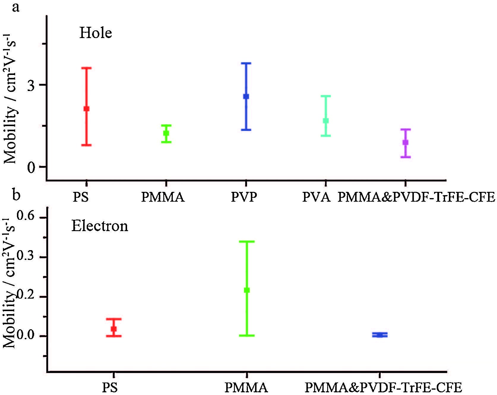
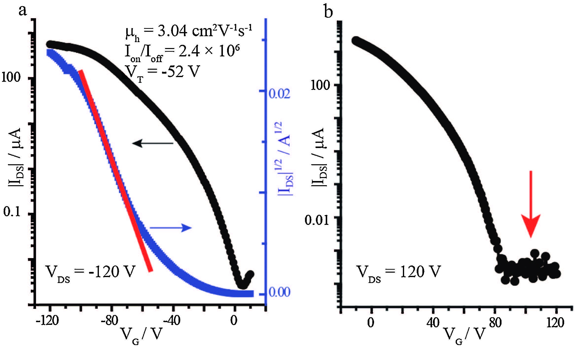
The typical transfer and output characteristics of TIPS- pentacene on PMMA,PS and PMMA&P(VDF-TrFE-CFE) dielectrics have been shown in Fig. 3,exhibiting obvious electron transport. For every device,n-channel behavior was observed in addition to their π-channel behavior,with the FET parameters summarized in Table 1and Fig. 4. For PS(Fig. 3e-h),an average electron mobility(me) of 0.036 ±0.025 cm2 V-h-1 (range: 0.00073-0.087 cm2 V-1s-1),on-to-off current ratios (Ion/Ioff)〜102,and threshold voltages (VT) between 78 and 98 V were obtained. For PMMA (Fig. 3a-d),an average electronmobility(me)of0.23±0.13cm2V-1s-1(range:0.0035- 0.48 cm2 V-1 s-1),on-to-off current ratios (Ion/Ioff)〜101,and threshold voltages (VT) between 72 V and 94 V were obtained as well. The slightly higher electron mobility on PMMA is attributed to the more smooth morphology of the crystals than that on PS dielectric,as shown by AFM (Fig. 2k,l,p,q). In comparison,crystals grown on PMMA&P(VDF-TrFE-CFE) surfaces show worse n-channel behavior (Fig. 3i-l),with only 37 devices (out of 50) exhibiting electron transport. And the achieved electron mobility is lower,with an average value of 0.0059 ± 0.0075 cm2 V-1 s-1 (range: 0.00044-0.0034 cm2 V-1 s-1). The lower mobility in the case of PMMA&P(VDF-TrFE-CFE) surfaces is attributed to the strong surface polarization effects originated from the high-k dielectric of P(VDF-TrFE-CFE) [36, 66].
In sharp contrast,the crystals grown on PVP dielectric show no electron transport (Fig. 5b,red arrow) but only hole transport (Fig. 5a). The suppressed electron transport is attributed to the hydroxyl groups on the PVP that has been demonstrated to heavily trap electrons [33]. Consistently,the crystals grown on PVA (1 mg/mL) dielectric that contains hydroxyl groups as well exhibit unipolar behavior without electron transport (Fig. 6a and b,red arrow). Interestingly,as we increased the thickness of the PVA dielectric films from 2 nm to 40 nm,we observed electron transport (Fig. 6c-f). An average electron mobility (me) of 0.038 ±0.041 cm2 V-1s-1 (range: 0.00085-0.14 cm2 V-1s-1), on-to-off current ratios (Ion/Ioff) ~102,and threshold voltages (VT) between 63 V and 92 V were obtained. This unipolar to ambipolar transition was previously reported in another typical π-channel molecule,pentacene [41, 42, 67, 68]. Similarly,hole transport was only observed for pentacene on PVA dielectric of 100 nm thick,while additional electron transport emerged for pentacene on thick PVA films (600 nm). As proved by Takebayashi et al.,the emerging electron transport is due to the Na+ ions in PVA,which is introduced by synthesis process. The Na+ ions change the character of the injection barrier at the Au/semiconductor junction and enable the n-type operation. This phenomenon reveals that electron transport is possible even on the hydroxyl-rich surfaces.

|
Download:
|
| Figure 4. Hole (a) and electron (b) mobility of TIPS-pentacene single crystals on various polymer dielectrics. | |

|
Download:
|
| Figure 5. FET characteristics of TIPS-pentacene single-crystals grown on PVP. Typical transfer of the FETs in p-channel operation (a) and n-channel operation (b)[1TD$DIF]. | |

|
Download:
|
| Figure 6. FET characteristics of TIPS-pentacene single-crystals grown on PVA (1 mg/ mL) (a,b) and PVA (10mg/mL) (c-f),respectively. (a-d) Typical transfer characteristics of FET in π- (a,c) and n- (b,d) channel operation mode. (e,f) Output characteristics of FET in π- (e) and n- (f) channel operation mode. | |
3.2. The effect of polar impurities on electron transport
Next,we examined the effect of polar impurities to the electron transport. 15 devices based on TIPS-pentacene single crystals grown on PMMA were exposed for 2 min (Fig. 7a) to the vapor of a variety of polar molecules including CHCl3,CH2Cl2,1,2-DCE and THF,and the FET performance before and after the vapor exposure was compared. After being exposed to the CHCl3 vapor,the electron mobility sharply drops (Fig. 7b,green line) from 0.15 cm2 V-1 s-1 to 0.0074 cm2 V-1 s-1. Because the morphology of the PMMA dielectric and single crystals were little changed after treated in CHCl3 vapor (Fig. 7c and d),the reduced electron mobility is not due to the erosion of the PMMA and TIPS-pentacene single crystals. Instead,the lowered mobility is attributed to the incorporation of trace amount of CHCl3 near the conduction channels. Similar to the surface polarization effects of the dielectrics [33, 57-59],the incorporated CHCl3 molecules,as polarizable sources [69],will introduce dipolar disorder to the FET channels and lead to reduced electron mobility. As a supporting evidence for the CHCl3 incorporation,the reduced electron transport partially recovered to 0.03 cm2 V-1 s-1 after the devices were heated for 2 h at 80 ℃ in the N2 glovebox (Fig. 7b,blue line). Consistently,exposure to other polar vapors of CH2Cl2,1,2-DCE and THF did not change the morphology of the PMMA dielectric and single crystals (Fig. S3 in Supporting Information),but greatly reduced electron mobility (Fig. 8 and Fig. S4 in Supporting information). Also,the reduced mobility partially recovered after heat treatment to remove the polar impurities.

|
Download:
|
| Figure 7. (a) Schematic representations of the method to treat the crystals with polar solvent vapor. (b) Sqrt (IDS) vs. VG curves of the as-prepared, CHCl3-treated and heat-treated TIPS-pentacene single crystals, and the electron mobility calculated from each curve has been marked. Inset: Comparison of transfer characteristics among the as-prepared, CHCl3-treated and heat-treated crystals. (c, d) AFM images of PMMA dielectric and TIPS-pentacene treated by CHCl3 vapor, respectively. | |

|
Download:
|
| Figure 8. Statistical charts of electron mobility treated by polar solvent, including CHCl3 (a), CH2Cl2 (b), 1,2-DCE (c) and THF (d), and heating. | |
4. Conclusion
In summary,we have demonstrated the effect of gate dielectrics and polar impurities on the electron transport in TIPS-pentacene single crystals. Electron transport emerges in the crystals on PMMA,PS,and a bilayer dielectric of PMMA on P(VDF-TrFE-CFE),confirming the recently reported unusual electron transport of TIPS-pentacene single crystals on BCB dielectric. In contrast,electron transport is suppressed in the crystals on PVP,in consistent with the known trap effect of hydroxyl groups (in PVP). Electron transport of the crystals on PVA depends on the PVA thickness and,on thick one of 40 nm,the electron mobility reaches as high as 0.14 cm2 V-1 s-1. Among these five dielectrics,the highest electron mobility of 0.48 cm2 V-1 s-1 has been achieved in the crystals on PMMA,which is attributed to hydroxyl-free and relatively low-k value of the PMMA dielectric as well as the smooth crystal morphology. In addition,the electron transport is sensitive to the polar impurities. Exposure to the vapor of a variety of polar solvents including CHCl3,CH2Cl2,1,2-DCE and THF results in dramatically reduced electron mobility. These results have the potential to lead to design criteria for n-channel and ambipolar OFETs.
Appendix A. Supplementary dataSupplementary data associated with this article can be found,in the online version,at http://dx.doi.org/10.1016/jxclet.2016.05.016.
Acknowledgments This work was supported by the 973 Program (No. 2014CB643503),National Natural Science Foundation of China (Nos. 51373150,51461165301),and Zhejiang Province Natural Science Foundation (No. LZ13E030002).| [1] | Gelinck G.H., Huitema H.E.A., van Veenendaal E., Flexible active-matrix displays and shift registers based on solution-processed organic transistors. Nat. Mater. 3 (2004) 106–110. DOI:10.1038/nmat1061 |
| [2] | Sekitani T., Yokota T., Zschieschang U., Organic nonvolatile memory transistors for flexible sensor arrays. Science 326 (2009) 1516–1519. DOI:10.1126/science.1179963 |
| [3] | Podzorov V., Menard E., Borissov A., Intrinsic charge transport on the surface of organic semiconductors. Phys. Rev. Lett. 93 (2004) 086602. DOI:10.1103/PhysRevLett.93.086602 |
| [4] | Sundar V.C., Zaumseil J., Podzorov V., Elastomeric transistor stamps:reversible probing of charge transport in organic crystals. Science 303 (2004) 1644–1646. DOI:10.1126/science.1094196 |
| [5] | Takeya J., Yamagishi M., Tominari Y., Very high-mobility organic singlecrystal transistors with in-crystal conduction channels. Appl. Phys. Lett. 90 (2007) 102120. DOI:10.1063/1.2711393 |
| [6] | Jurchescu O.D., Popinciuc M., van Wees B.J., Palstra T.T.M., Interface-controlled, high-mobility organic transistors. Adv. Mater. 19 (2007) 688–692. DOI:10.1002/(ISSN)1521-4095 |
| [7] | Minemawari H., Yamada T., Matsui H., Inkjet printing of single-crystal films. Nature 475 (2011) 364–367. DOI:10.1038/nature10313 |
| [8] | Li J., Zhao Y., Tan H.S., A stable solution-processed polymer semiconductor with record high-mobility for printed transistors. Sci. Rep. 2 (2012) 754. |
| [9] | Diao Y., Tee B.C.K., Giri G., Solution coating of large-area organic semiconductor thin films with aligned single-crystalline domains. Nat. Mater. 12 (2013) 665–671. DOI:10.1038/nmat3650 |
| [10] | Kang I., Yun H.J., Chung D.S., Kwon S.K., Kim Y.H., Record high hole mobility in polymer semiconductors via side-chain engineering. J. Am. Chem. Soc. 135 (2013) 14896–14899. DOI:10.1021/ja405112s |
| [11] | Yuan Y.B., Giri G., Ayzner A.L., Ultra-high mobility transparent organic thin film transistors grown by an off-centre spin-coating method. Nat. Commun. 5 (2014) 3005. |
| [12] | Luo C., Kyaw A.K.K., Perez L.A., General strategy for self-assembly of highly oriented nanocrystalline semiconducting polymers with high mobility. Nano Lett. 14 (2014) 2764–2771. DOI:10.1021/nl500758w |
| [13] | Kim G., Kang S.J., Dutta G.K., A thienoisoindigo-naphthalene polymer with ultrahigh mobility of 14.4 cm2/V·s that substantially exceeds benchmark values for amorphous silicon semiconductors. J. Am. Chem. Soc. 136 (2014) 9477–9483. DOI:10.1021/ja504537v |
| [14] | Back J.Y., Yu H., Song I., Investigation of structure-property relationships in diketopyrrolopyrrole-based polymer semiconductors via side-chain engineering. Chem. Mater. 27 (2015) 1732–1739. DOI:10.1021/cm504545e |
| [15] | Liu J., Zhang H.T., Dong H.L., High mobility emissive organic semiconductor. Nat. Commun. 6 (2015) 10032. DOI:10.1038/ncomms10032 |
| [16] | Li H.Y., Tee B.C.K., Cha J.J., High-mobility field-effect transistors from largearea solution-grown aligned C60 single crystals. J. Am. Chem. Soc. 134 (2012) 2760–2765. DOI:10.1021/ja210430b |
| [17] | Lee J., Han A.R., Yu H., Boosting the ambipolar performance of solutionprocessable polymer semiconductors via hybrid side-chain engineering. J. Am. Chem. Soc. 135 (2013) 9540–9547. DOI:10.1021/ja403949g |
| [18] | Sun B., Hong W., Yan Z.Q., Aziz H., Li Y.N., Record high electron mobility of 6.3 cm2 V-1 s-1 achieved for polymer semiconductors using a new building block. Adv. Mater. 26 (2014) 2636–2642. DOI:10.1002/adma.v26.17 |
| [19] | Yun H.J., Kang S.J., Xu Y., Dramatic inversion of charge polarity in diketopyrrolopyrrole-based organic field-effect transistors via a simple nitrile group substitution. Adv. Mater. 26 (2014) 7300–7307. DOI:10.1002/adma.v26.43 |
| [20] | Liu D.Q., He Z.K., Su Y.R., Self-assembled monolayers of cyclohexyl-terminated phosphonic acids as a general dielectric surface for high-performance organic thin-film transistors. Adv. Mater. 26 (2014) 7190–7196. DOI:10.1002/adma.v26.42 |
| [21] | He T., Stolte M., Burschka C., Single-crystal field-effect transistors of new Cl2-NDI polymorph processed by sublimation in air. Nat. Commun. 6 (2015) 5954. DOI:10.1038/ncomms6954 |
| [22] | Dou J.H., Zheng Y.Q., Yao Z.F., A cofacially stacked electron-deficient small molecule with a high electron mobility of over 10 cm2 V-1 s-1 in air. Adv. Mater. 27 (2015) 8051–8055. DOI:10.1002/adma.201503803 |
| [23] | Dou J.H., Zheng Y.Q., Yao Z.F., Fine-tuning of crystal packing and charge transport properties of BDOPV derivatives through fluorine substitution. J. Am. Chem. Soc. 137 (2015) 15947–15956. DOI:10.1021/jacs.5b11114 |
| [24] | Xue G.B., Wu J.K., Fan C.C., Boosting the electron mobility of solution-grown organic single crystals via reducing the amount of polar solvent residues. Mater. Horiz. 3 (2016) 119–123. DOI:10.1039/C5MH00190K |
| [25] | Zhang F.J., Hu Y.B., Schuettfort T., Critical role of alkyl chain branching of organic semiconductors in enabling solution-processed N-channel organic thinfilm transistors with mobility of up to 3.50 cm2 V-1 s-1. J. Am. Chem. Soc. 135 (2013) 2338–2349. DOI:10.1021/ja311469y |
| [26] | Crone B., Dodabalapur A., Lin Y.Y., Large-scale complementary integrated circuits based on organic transistors. Nature 403 (2000) 521–523. DOI:10.1038/35000530 |
| [27] | Tang C.W., Two-layer organic photovoltaic cell. Appl. Phys. Lett. 48 (1986) 183–185. DOI:10.1063/1.96937 |
| [28] | Tang C.W., VanSlyke S.A., Organic electroluminescent diodes. Appl. Phys. Lett. 51 (1987) 913–915. DOI:10.1063/1.98799 |
| [29] | Newman C.R., Frisbie C.D., da Silva Filho D.A., Introduction to organic thin film transistors and design of n-channel organic semiconductors. Chem. Mater. 16 (2004) 4436–4451. DOI:10.1021/cm049391x |
| [30] | Zaumseil J., Sirringhaus H., Electron and ambipolar transport in organic fieldeffect transistors. Chem. Rev. 107 (2007) 1296–1323. DOI:10.1021/cr0501543 |
| [31] | de Leeuw D.M., Simenon M.M.J., Brown A.R., Einerhand R.E.F., Stability of n-type doped conducting polymers and consequences for polymeric microelectronic devices. Synth. Met. 87 (1997) 53–59. DOI:10.1016/S0379-6779(97)80097-5 |
| [32] | Di Pietro R., Fazzi D., Kehoe T.B., Sirringhaus H., Spectroscopic investigation of oxygen- and water-induced electron trapping and charge transport instabilities in n-type polymer semiconductors. J. Am. Chem. Soc. 134 (2012) 14877–14889. DOI:10.1021/ja304198e |
| [33] | Chua L.L., Zaumseil J., Chang J.F., General observation of n-type field-effect behaviour in organic semiconductors. Nature 434 (2005) 194–199. DOI:10.1038/nature03376 |
| [34] | Bussac M.N., Picon J.D., Zuppiroli L., The impact of molecular polarization on the electronic properties of molecular semiconductors. Europhys. Lett. 66 (2004) 392–398. DOI:10.1209/epl/i2003-10218-8 |
| [35] | Valeev E.F., Coropceanu V., da Silva Filho D.A., Salman S., Bré das J.L., Effect of electronic polarization on charge-transport parameters in molecular organic semiconductors. J. Am. Chem. Soc. 128 (2006) 9882–9886. DOI:10.1021/ja061827h |
| [36] | Minder N.A., Ono S., Chen Z.H., Facchetti A., Morpurgo A.F., Band-like electron transport in organic transistors and implication of the molecular structure for performance optimization. Adv. Mater. 24 (2012) 503–508. DOI:10.1002/adma.201103960 |
| [37] | Anthony J.E., Facchetti A., Heeney M., Marder S.R., Zhan X.W., n-type organic semiconductors in organic electronics. Adv. Mater. 22 (2010) 3876–3892. DOI:10.1002/adma.200903628 |
| [38] | Zhao Y., Guo Y.L., Liu Y.Q., 25th anniversary article:recent advances in n-type and ambipolar organic field-effect transistors. Adv. Mater. 25 (2013) 5372–5391. DOI:10.1002/adma.201302315 |
| [39] | Mei J.G., Diao Y., Appleton A.L., Fang L., Bao Z.N., Integrated materials design of organic semiconductors for field-effect transistors. J. Am. Chem. Soc. 135 (2013) 6724–6746. DOI:10.1021/ja400881n |
| [40] | Debucquoy M., Rockelé M., Genoe J., Gelinck G.H., Heremans P., Charge trapping in organic transistor memories:on the role of electrons and holes. Org. Electron. 10 (2009) 1252–1258. DOI:10.1016/j.orgel.2009.07.005 |
| [41] | Singh T.B., Meghdadi F., Günes S., High-performance ambipolar pentacene organic field-effect transistors on poly(vinyl alcohol) organic gate dielectric. Adv. Mater. 17 (2005) 2315–2319. DOI:10.1002/(ISSN)1521-4095 |
| [42] | Singh T.B., Senkarabacak P., Sariciftci N.S., Organic inverter circuits employing ambipolar pentacene field-effect transistors. Appl. Phys. Lett. 89 (2006) 033512. DOI:10.1063/1.2235947 |
| [43] | Xu X.M., Xiao T., Gu X., Solution-processed ambipolar organic thin-film transistors by blending p- and n-type semiconductors:solid solution versus microphase separation. ACS Appl. Mater. Interfaces 7 (2015) 28019–28026. DOI:10.1021/acsami.5b01172 |
| [44] | Rost C., Karg S., Riess W., Ambipolar light-emitting organic field-effect transistor. Appl. Phys. Lett. 85 (2004) 1613–1615. DOI:10.1063/1.1785290 |
| [45] | Wang J., Wang H.B., Yan X.J., Heterojunction ambipolar organic transistors fabricated by a two-step vacuum-deposition process. Adv. Funct. Mater. 16 (2006) 824–830. DOI:10.1002/(ISSN)1616-3028 |
| [46] | Fan C.C., Zoombelt A.P., Jiang H., Solution-grown organic single-crystalline p-n junctions with ambipolar charge transport. Adv. Mater. 25 (2013) 5762–5766. DOI:10.1002/adma.v25.40 |
| [47] | Zhang Y.J., Dong H.L., Tang Q.X., Organic single-crystalline p-n junction nanoribbons. J. Am. Chem. Soc. 132 (2010) 11580–11584. DOI:10.1021/ja102779x |
| [48] | Dodabalapur A., Katz H.E., Torsi L., Haddon R.C., Organic heterostructure field-effect transistors. Science 269 (1995) 1560–1562. DOI:10.1126/science.269.5230.1560 |
| [49] | Qin Y.K., Zhang J., Zheng X.Y., Charge-transfer complex crystal based on extended-p-conjugated acceptor and sulfur-bridged annulene:charge-transfer interaction and remarkable high ambipolar transport characteristics. Adv. Mater. 26 (2014) 4093–4099. DOI:10.1002/adma.v26.24 |
| [50] | Xue G.B., Fan C.C., Wu J.K., Ambipolar charge transport of TIPS-Pentacene single-crystals grown from non-polar solvents. Mater. Horiz. 2 (2015) 344–349. DOI:10.1039/C4MH00211C |
| [51] | Anthony J.E., Brooks J.S., Eaton D.L., Parkin S.R., Functionalized pentacene:Improved electronic properties from control of solid-state order. J. Am. Chem. Soc. 123 (2001) 9482–9483. DOI:10.1021/ja0162459 |
| [52] | Payne M.M., Parkin S.R., Anthony J.E., Kuo C.C., Jackson T.N., Organic field-effect transistors from solution-deposited functionalized acenes with mobilities as high as 1 cm2/V·s. J. Am. Chem. Soc. 127 (2005) 4986–4987. DOI:10.1021/ja042353u |
| [53] | Kim D.H., Lee D.Y., Lee H.S., High-mobility organic transistors based on single-crystalline microribbons of triisopropylsilylethynyl pentacene via solution-phase self-assembly. Adv. Mater. 19 (2007) 678–682. DOI:10.1002/(ISSN)1521-4095 |
| [54] | Hamilton R., Smith J., Ogier S., High-performance polymer-small molecule blend organic transistors. Adv. Mater. 21 (2009) 1166–1171. DOI:10.1002/adma.v21:10/11 |
| [55] | Giri G., Verploegen E., Mannsfeld S.C.B., Tuning charge transport in solutionsheared organic semiconductors using lattice strain. Nature 480 (2011) 504–508. DOI:10.1038/nature10683 |
| [56] | Liu S., Wu J.K., Fan C.C., Large-scale fabrication of field-effect transistors based on solution-grown organic single crystals. Sci. Bull. 60 (2015) 1122–1127. DOI:10.1007/s11434-015-0817-9 |
| [57] | Veres J., Ogier S.D., Leeming S.W., Cupertino D.C., Khaffaf S.M., Low-k insulators as the choice of dielectrics in organic field-effect transistors. Adv. Funct. Mater. 13 (2003) 199–204. DOI:10.1002/adfm.200390030 |
| [58] | Stassen A.F., de Boer R.W.I., Iosad N.N., Morpurgo A.F., Influence of the gate dielectric on the mobility of rubrene single-crystal field-effect transistors. Appl. Phys. Lett. 85 (2004) 3899–3901. DOI:10.1063/1.1812368 |
| [59] | Hulea I.N., Fratini S., Xie H., Tunable Frö hlich polarons in organic singlecrystal transistors. Nat. Mater. 5 (2006) 982–986. DOI:10.1038/nmat1774 |
| [60] | Khim D., Xu Y., Baeg K.J., Large enhancement of carrier transport in solutionprocessed field-effect transistors by fluorinated dielectric engineering. Adv. Mater. 28 (2016) 518–526. DOI:10.1002/adma.v28.3 |
| [61] | Chung T.C., Petchsuk A., Synthesis and properties of ferroelectric fluoroterpolymers with curie transition at ambient temperature. Macromolecules 35 (2002) 7678–7684. DOI:10.1021/ma020504c |
| [62] | Li J.H., Sun Z.H., Yan F., Solution processable low-voltage organic thin film transistors with high-k relaxor ferroelectric polymer as gate insulator. Adv. Mater. 24 (2012) 88–93. DOI:10.1002/adma.201103542 |
| [63] | Li H.Y., Tee B.C.K., Giri G., High-performance transistors and complementary inverters based on solution-grown aligned organic single-crystals. Adv. Mater. 24 (2012) 2588–2591. DOI:10.1002/adma.v24.19 |
| [64] | Li H.Y., Fan C.C., ${referAuthorVo.mingEn} M.Vosgueritchian, Tee B.C.K., Chen H.Z., Solution-grown aligned C60 single-crystals for field-effect transistors. J. Mater. Chem. C 2 (2014) 3617–3624. DOI:10.1039/c3tc32431a |
| [65] | Huang Z.T., Fan C.C., Xue G.B., Solution-grown aligned crystals of diketopyrrolopyrroles (DPP)-based small molecules:rough surfaces and relatively low charge mobility. Chin. Chem. Lett. 27 (2016) 523–526. DOI:10.1016/j.cclet.2016.01.054 |
| [66] | Coropceanu V., Bré das J.L., Organic transistors:a polarized response. Nat. Mater. 5 (2006) 929–930. DOI:10.1038/nmat1791 |
| [67] | Takebayashi S., Abe S., Saiki K., Ueno K., Origin of the ambipolar operation of a pentacene field-effect transistor fabricated on a poly(vinyl alcohol)-coated Ta2O5 gate dielectric with Au source/drain electrodes. Appl. Phys. Lett. 94 (2009) 083305. DOI:10.1063/1.3089692 |
| [68] | Chang J.W., Hsu W.L., Wu C.Y., Guo T.F., Wen T.C., The polymer gate dielectrics and source-drain electrodes on n-type pentacene-based organic field-effect transistors. Org. Electron. 11 (2010) 1613–1619. DOI:10.1016/j.orgel.2010.07.003 |
| [69] | Borsenberger P.M., Bässler H., Concerning the role of dipolar disorder on charge transport in molecularly doped polymers. J. Chem. Phys. 95 (1991) 5327–5331. DOI:10.1063/1.461646 |