 2016, Vol. 27


b University of Chinese Academy of Sciences, Beijing 100049, China
Owing to the peculiarities of low cost,light weight,mechanical flexibility,large-area capability,and ease of fabrication,organic photovoltaics (OPVs) have attracted much attention over the past two decades [1-7]. Recent efforts have pushed the power conversion efficiencies (PCEs) exceeding 10% for both polymerbased [8, 9] and small molecule-based [10-14] organic solar cells (OSCs) employing a single photoactive layer. Nevertheless,it still does not reach commercial viability. In general,the active layer consists of two distinct components of electron-rich donor (D) and electron-deficient acceptor (A) materials with a bilayer or bulk heterojunction architecture. In order to achieve an efficient OPV operation,a series of successive electronic processes must be optimized within the active layer,including (1) exciton formation by sunlight absorption in D and/or A materials,(2) exciton diffusion to the D/A interface before decaying to the ground state,(3) exciton dissociation (ED) into charge-transfer (CT) states at the D/A interface,where hole and electron are still weakly electrostatically bounded,(4) hole and electron separation into free charge carriers and migration along D and A toward the anode and cathode,respectively,and (5) finally hole and electron collection at the respective electrode [2, 15, 16]. In the meanwhile ,the undesirable (geminate,bimolecular,trap-assisted,etc.) charge recombination (CR) processes must be prevented,thus requiring a fine balancing act.
Critical to these key processes are the molecular packing configurations in the active layer,especially the D/A intermolecular arrangements at the interface [15-22]. Recent quantum-chemical studies on model constructed and molecular dynamics (MD) simulatedD/Acomplexespointedout that,the competitionbetween ED and geminate CR is closely relevant to the interfacial packing [17, 23, 24]. Except the exquisite interface engineering,the impact of hot CT states in the ED process has also been emerged [23, 25-27]. Some recent experiments revealed that hot CT excitons could dissociate into free charge carriers within several hundreds of femtoseconds before decaying into the lowest CT (CT0) state [25- 27]. These will be the focus of Section 2 where we take the example of DTDCTB/C60 complexes to clarify the EDand CRmechanisms [23]. The OSCs based on DTDCTB/fullerene heterojunctions have been widely investigated and achieved a relatively high PCE of exceeding 8% [28-39]. Importantly,our calculations pointed to that hot CT statesdominate theEDprocess intheDTDCTB/C60 complexes,which is favorable to obtain ultrafast charge separation.
Although modulation of the active layer morphologies for efficient generation of free carriers has been successfully achieved by several different preparation procedures [1, 19, 20, 40-43],it still remains very difficult to experimentally probe the molecular selfassembly processes and packing structures [44],especially the myriad morphologies available in the active layer. This will severely hinder obtaining reliable structure-property relationships and further improving the device performance. It is the reason why atomistic MD simulations are increasingly used as a powerful tool to obtain further understanding of the buried bulk and interfacial morphologies [24, 45-51],which will be the focus of Section 3. In this part,we summarize the modeling schemes of vapor-deposition and solution-processing processes and our two recent works. First,the impact of different DTDCTB surfaces on fullerene packing and interfacial morphologies are analyzed [24]. Second,the effect of solvent evaporation rate and thermal annealing on the molecular packing morphology and charge transport is unraveled for a diketopyrrolopyrrole (DPP)-based small-molecule donor material [51],DPP(TBFu)2 [52-55],which displays excellent hole mobility.
2. Excited-state charge-transfer processes at the donor/acceptor interface 2.1. MethodologyElectronic coupling between the local excited and chargetransfer states is one of the key parameters to evaluate the excitedstate charge-transfer processes at the donor/acceptor interface. Several methods have been developed to compute electronic couplings,such as the fragment molecular orbital (FMO) method [56],energy level splitting (ELS) method [57],generalized Mulliken-Hush (GMH) model [58],and constrained density functional theory (CDFT) [59]. The electronic couplings provided by the FMO and ELS methods are originated from the interaction between frontier molecular orbitals based on the single-electron approximation. The GMH model can deal with many-electron states,but it is applicable only when the adiabatic states are constructed by two diabatic states. For the method based on CDFT,just the ground CT state can be considered. Recently,a diabaticstate approach was developed,which can calculate electronic couplings between any local and any CT states [17]. It is expressed as follows:
| ${{V}_{ab}}=\left\langle \psi _{a}^{LE}\left| H \right|\psi _{a}^{CT} \right\rangle $ | (1) |
here,ψaLE denotes the ground state or the excited state located on D or A,and ψb CT represents the CT state of the D-A complex,which are constructed as spin-adapted anti-symmetrized products of the isolated D and A wavefunctions,
| $\psi _{ij}^{LE}\left( S,M \right)=\sum\limits_{{{M}_{i}}{{M}_{j}}}{C_{{{S}_{i}}{{M}_{i}}{{S}_{j}}{{M}_{j}}}^{SM}}\left| \psi _{i}^{D}\left( {{S}_{i}},{{M}_{i}} \right)\psi _{j}^{A}\left( {{S}_{j}},{{M}_{j}} \right) \right|$ | (2) |
| $\psi _{km}^{CT}\left( S,M \right)=\sum\limits_{{{M}_{k}}{{M}_{m}}}{C_{{{S}_{k}}{{M}_{m}}{{S}_{m}}{{M}_{m}}}^{SM}}\left| \psi _{k}^{D+}\left( {{S}_{k}},{{M}_{k}} \right)\psi _{m}^{A-}\left( {{S}_{m}},{{M}_{m}} \right) \right|$ | (3) |
here,S and M are the total spin and spin projection of the D-A complex. ψi D/A represents the ith excited state of the donor or acceptor with spin Si and spin projection Mi,and ψkD+/A- represents the positively-charged state of D or negatively-charged state of A. The Clebsch-Gordan coefficients (CSiMiSjMjSM ) ensure that the linear combination of the products of the isolated wavefunctions is the eigenfunction of the total spin. The isolated excited and charged states of D and A can be calculated by the intermediate neglect of differential overlap (INDO) Hamiltonian [60] coupled to a single configuration interaction (SCI) scheme. In our following work,the Mataga-Nishimoto potential was applied to describe the coulomb repulsion term [61, 62].
Considering the degeneracies of the excited states of C60 and the CT states,the effective electronic couplings (Veff) are calculated as follows [17]:
| $V_{eff}^{2}=\frac{1}{{{g}_{a}}}{{\sum\limits_{ij}{\left( {{\psi }_{ai}}\left| H \right|{{\psi }_{bj}} \right)}}^{2}}$ | (4) |
where ga is the multiplicity of the initial diabatic state,and ψai and ψbj are the initial and final degenerate diabatic states,respectively.
| ${{\kappa }_{ab}}=V_{ab}^{2}\sqrt{\frac{\pi }{\lambda {{\kappa }_{B}}T{{h}^{2}}}}\exp \left[ -\frac{{{\left( \Delta G+\lambda \right)}^{2}}}{4\lambda {{\kappa }_{B}}T} \right]$ | (5) |
here,Vab is the electronic coupling described above,λ the reorganization energy,ΔG the Gibbs free energy,kB the Boltzmann constant,£ the reduced Planck constant,and T the temperature (set to 298.15 K in our study). It should be noted that compared with the Marcus theory,a much more complicate full quantum approach has been developed to calculate a more accurate rate through taking account of the nuclear tunneling effect [64-68].
Reorganization energy,λ consists of internal (λint) and external (λext) contributions. λint for exciton dissociation can be evaluated as the total relaxation energies from their excited-state or groundstate geometries to ionic geometries,while for charge recombination it corresponds to the total relaxation energies from their ionic geometries to neutral geometries. In the case of flexible molecules,e.g. DTDCTB,the steric hindrance effect on λint can be very important in the solid state,and λint should be evaluated by a hybrid quantum mechanics/molecular mechanics (QM/MM) approach [69]. At present,it is still difficult to reliably estimate λext,which is regarded as a variable and set to 0.06∼0.20 eV in our study [70, 71].
When the entropy contribution is ignored,Gibbs free energy,DG is equal to the energy difference between the initial and final diabatic states,and the energy of the diabatic state is calculated as the sum of the total energies of the isolated states of D and A and the Coulomb energy between D and A. For the local states,D and A are neutral and the Coulomb energies between D and A can be neglected. Therefore,the energies of local excited states are approximate to the excitation energies of the isolated D and A. However,the energies of the CT states must take into consideration the Coulomb interaction and can be estimated as [17]
| ${{E}_{CT}}=IP+EA+{{E}_{Coul}}$ | (6) |
where IP and EA are the ionization potential of D and the electron affinity of A,respectively. ECoul is the Coulomb energy between the cation of D and anion of A,
| ${{E}_{Coul}}=\sum\nolimits_{d\in {{D}^{+}},a\in A}{\frac{{{q}_{d}}{{q}_{a}}}{4\pi {{\varepsilon }_{0}}\varepsilon {{r}_{da}}}}$ | (7) |
here,d and a represent the atoms in D and A,respectively. qd and qa denote their corresponding partial charges (they are calculated by an INDO Mulliken population analysis in our work) and rda is the distance between atoms d and a. e0 and e are dielectric constants of the vacuum and medium (set to 4 in our work),respectively.
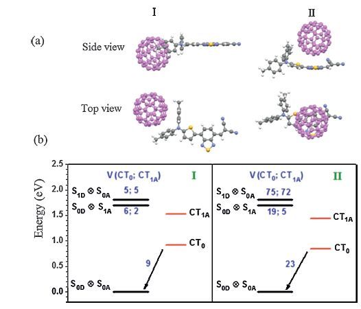
2.2. Exciton dissociation and charge recombination in DTDCTB/C60complexes 2.2.1. Energy alignments and electronic couplingsThe energy alignments and electronic couplings for the ED and CR processes in the DTDCTB/C60 complexes with different intermolecular orientations are shown in Fig. 1 [23]. The DTDCTB/C60 intermolecular geometries are optimized by DFTB3LYP/ 6-31G* with a Grimme’s D3 dispersion [72] (Fig. 1a). Two representative configurations I and II are considered with C60 near to the electron-donating and electron-withdrawing units,respectively. Besides the lowest CT state (CT0),another excited CT state (CT1A),which is originated from the first excitation of the negatively charged state of C60,is also involved in the ED process. The IP,EA,and S1 excitation energies of DTDCTB and C60 are taken from the experimental measurements in solid state [28, 73]. Along with the calculated Coulomb energies and excitation energies of the charge states,the energies of CT0 and CT1A are respectively estimated to be 0.92/0.84 and 1.52/1.44 eV in configuration I/II,which are lower than the S1 energy levels of DTDCTB and C60. DG for ED from S1D/S1A to CT0 and CT1A are then evaluated to be -0.89/-0.78 and -0.29/-0.18 eV in configuration I,while the corresponding values are 0.08 eV larger for configuration II. ΔG for the CR process is -0.92 and -0.84 eV for configuration I and II,respectively.

|
Download:
|
| Figure 1. The intermolecular geometries I and II of DTDCTB/C60 complexes (a) and electronic couplings for ED (from the local S1 states on DTDCTB and C60 to the lowest and excited CT states) and CR (from the lowest CT state to the ground state) processes along with the interfacial energy alignments of configuration I and II. Adapted from Shen et al. [23]. | |
As shown in Fig. 1b,the electronic couplings are much related to the interfacial orientations. The electronic couplings involving the local S1 states of DTDCTB and C60 are denoted as VS1D and VS1A,respectively. Because C60 is closer to the backbone of DTDCTB,configuration II exhibits much stronger electronic couplings for both ED and CR with respect to configuration I. In addition,VS1D involving both CT0 and CT1A states are much larger than VS1A in configuration II,whereas they are comparable in configuration I. Before the excited CT states recombine,they usually first relax into the CT0 state. Thus charge recombination will take place from the CT0 state. The electronic coupling for CR (VCR) is larger than both VS1D and VS1A in configuration I,while it is between VS1D and VS1A in configuration II.
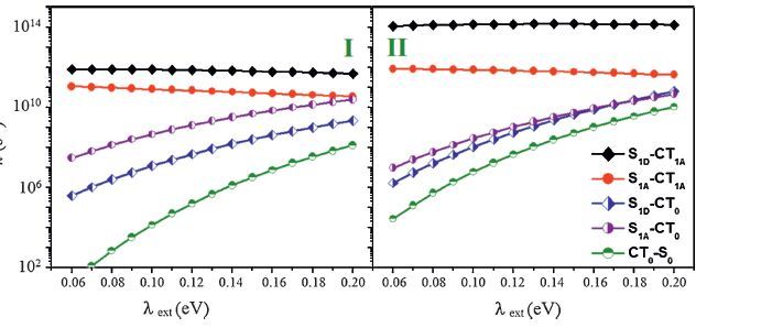
2.2.2. . Exciton-dissociation and charge-recombination ratesUsing the above electronic couplings and DG along with the calculated λint (which is 0.203 and 0.194 eV for ED involving S1D and S1A and 0.137 eV for CR,respectively),the electron-transfer rates are estimated according to Eq. (5). As shown in Fig. 2,the calculated CR rates are several orders of magnitude lower than the ED rates for both configurations. The CR rates are ∼102 -108 s-1 in configuration I while can reach ∼104-1010 s-1 in configuration II due to larger electronic couplings and more favorable driving forces. It is clear that the CR rates in configurations I and II are mostly below 109 s-1 and consistent with the experimental measurements,demonstrating that the time scale of CR is over sub-ns and ns.

|
Download:
|
| Figure 2. The calculated rates of exciton dissociation from the S1 states on DTDCTB and C60 to the CT0 and CT1A states,and of charge recombination from the CT0 state to the ground state for configurations I and II. The corresponding parameters for calculating rates are from experimental values: the energy of S1 state is 1.81 eV for DTDCTB and 1.70 eV for C60,IP (DTDCTB) = 5.3 eV,EA (C60) = -4.0 eV. Adapted from Shen et al. [23]. | |
In spite of different interface geometries,the dissociation rates of the C60-based excitons involving the CT0 state are lower than 1011 s-1. The DTDCTB-based excitons exhibit comparable and even lower dissociation rates in configuration I. Such exciton dissociation rates are in contrast to the experimental observation of ultrafast charge generation. Strikingly,for the ED process involving the CT1A state,the rates can reach ∼1011 and 1012 s-1 in configuration I and even as high as ∼1012 and 1014 s-1 in configuration II for the C60 and DTDCTB-based excitons,respectively. These calculated rates are in good agreement with the time scale of ultrafast charge separation (∼100 fs) measured by experiments. Thus,our calculations indicate that the hot CT states determine the exciton dissociation processes in the DTDCTB/C60 complex. Additionally,interface geometries can have an important impact on the electron-transfer processes at the D/A interface. It should be noted that thatmore complicated complexes consisting of more donor and acceptor molecules need to be considered to providemore reliable interface geometries aswell as aggregations of donor and acceptor that would result in electronic delocalization.
3. Molecular dynamics simulations of the active-layer morphologies 3.1. Modelling schemes of vapor deposition and solution processing proceduresCurrently,the active layers of OSCs are often fabricated via vapor deposition or solution processing procedures [1]. The interfacial or bulk morphologies for OSCs have been investigated through equilibrium MD simulations [47-50]. In this scheme,pure D and A phases,which are derived from crystal structures or random arrangements,are first merged together and then equilibrated by MD simulations. Brédas et al. have delineated how the nature of the pentacene surfaces,i.e. (0 0 1) or (0 1 0),influences the interfacial packing configurations with a lot of fullerenes randomly distributed on the ‘pristine’ pentacene surfaces at one time [48]. It is found that the deposited fullereneswouldflock together and settle downonthe surface very soon without adequate time to self-organize. Recently,Muccioli et al. developed a quasi-equilibriumapproach inwhich the active molecules are one-by-one consecutively deposited on the substrate surface to mimic the vapor deposition process. Using this scheme,they have successfully studied the crystal growth of pentacene or sexithiophene on the C60(0 0 1) substrate [45, 46]. However,the relationship between different surface properties and thin-film morphologies is yet to be revealed. Moreover,in conventional bilayer devices,the C60 layer residues on the top of the donor layer. Therefore,it is very interesting to investigate the influence of donor surfaces with different features on the fullerene packing and interfacial morphology using the quasi-equilibrium approach,whichwill be discussed taking the DTDCTB/C60 system as an example in Section 3.2.
The solution-processing process could also be modeled in the framework of quasi-equilibrium MD simulations [51, 74]. At the first step,a solution containing active molecules and solvent molecules is constructed and equilibrated. Then a certain amount of solvent molecules are randomly removed at a predefined time dt to model solvent evaporation. After all the solvents disappear,a dried film is well fabricated. The evaporation rate can be controlled by varying the value of dt. Furthermore,the effect of thermal annealing (TA) treatment on molecular packing can be studied based on the as-cast film. In vey recent,we have investigated the effect of the solvent evaporation rate and TA on the molecular packing and ordering of a small-molecule donor material DPP(TBFu)2 [51],which is to be presented in Section 3.3.
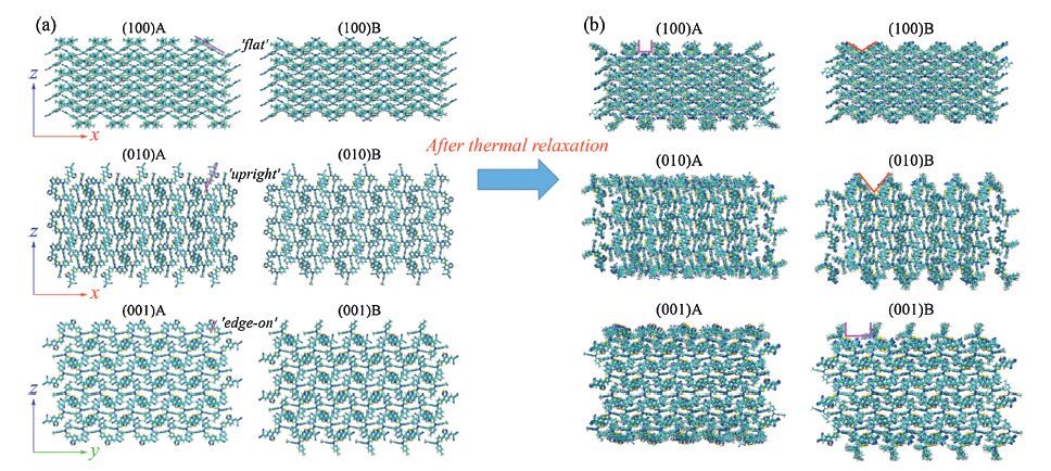
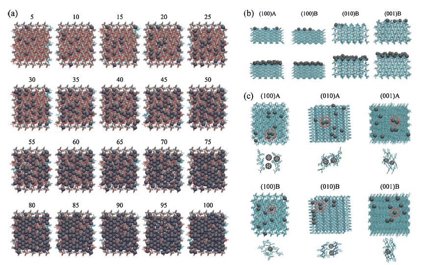
3.2. Deposition growth and morphologies of C60 on DTDCTB surfacesTo develop slab models for deposition of C60,supercells with the sizes of 5×5×5 (8.47×9.18×3.84 nm3 ,500 molecules),5×12×3 (9.18×9.21×5.08 nm3,720 molecules),and 12×5×3 (9.21×8.47×5.51 nm3,720 molecules) are built by replication of the unit cell of the DTDCTB crystal for the (1 0 0),(0 1 0),and (0 0 1) surfaces,respectively (Fig. 3a). The supercell periodicity was maintained in the xy plane while the z-direction was elongated to 20 nm to produce a vacuum layer. It should be mentioned that the size of supercell (surface size and film thickness) could influence the dynamics of C60 growth. Here,the surface size (∼ 9×9 nm2) can accommodate at least 80 C60 molecules and is large enough for exploring the C60 aggregation behaviors on the surface. Each type of slab has two different facets,labeled as A and B (i.e. obtained by cutting the cell at full and half cell,respectively),because of an antiparallel packing mode in the DTDCTB crystal [28]. Obviously,the initial surfaces show different molecular orientations,i.e. nearly ‘flat’,‘upright’ and ‘edge-on’ configurations. These initial slabs were then fully equbilibrated at room temperature to achieve relaxed substrate surfaces. During the thermal relaxation,the molecules in the middle layers hold relatively stable,indicating the thickness of these slabs is reasonable. Interestingly,after thermal relaxation,the intermolecular arrangement on the (1 0 0)A surface exhibits a collective reorientation,while the (0 1 0)A and (0 0 1)A surfaces become very disordered and form amorphous conformations (Figs. 3b and 4a). In contrast,all the B surfaces keep relatively stabilized with only some dynamic disorders.

|
Download:
|
| Figure 3. (a) Depictions of the DTDCTB (1 0 0),(0 1 0) and (0 0 1) slabs derived from the DTDCTB crystal structure. Each lattice has two opposite faces,labeled as A and B. (b) Illustration of the relaxed DTDCTB surfaces. Adapted from Han et al. [24]. | |

|
Download:
|
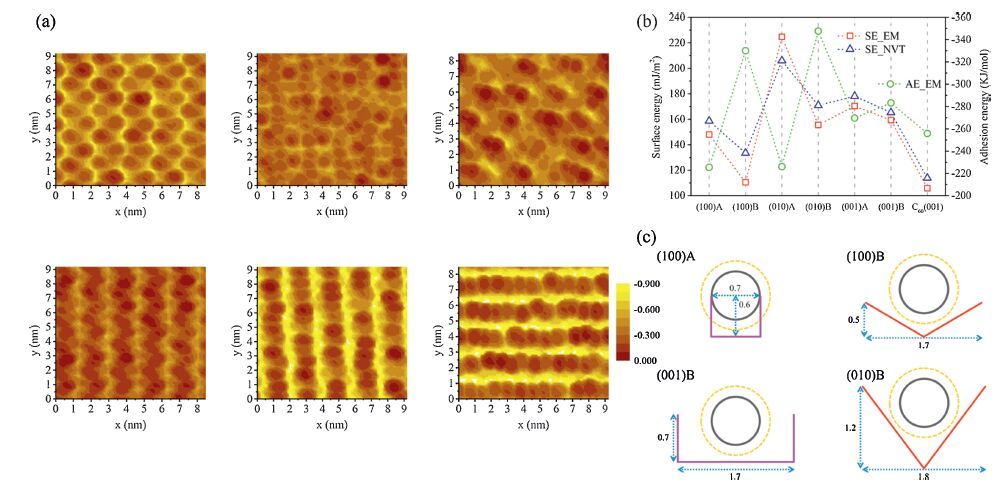
| Figure 4. (a) The topography maps for the relaxed DTDCTB surfaces using the C60 molecule as an AFM tip (the highest point is referenced as the zero point for each surface ). (b) Calculated surface energies (SE) via energy minimization (EM) and NVT equilibration and adhesion energies (AE) via EM for the different DTDCTB surfaces and the C60(0 0 1) surface. (c) Schematic diagrams of the surface furrows for the ordered DTDCTB (1 0 0)A and (0 0 1)B (pink) as well as (1 0 0)B and (0 1 0)B (red) surfaces. The length unit is nm. The gray circle represents size of the C60 nuclear cage,and the brown dotted circle indicates the size of the C60 cage considering the van der Waals radius of the carbon atom. Adapted from Han et al. [24]. | |
By means of the quasi-equilibrium molecular dynamics,400 C60 molecules were one-by-one consecutively deposited at every 100 ps on the relaxed surfaces. Fig. 5 shows some pictures of the intermediate processes and packing structures. Although this frequency is much high relative to experiment,the time interval for each deposition is big enough for C60 to self-assemble. After deposition,each bilayer was equilibrated at room temperature for 10 ns. The ultimate bilayer morphologies and DTDCTB/C60 interfacial configurations are displayed in Fig. 6a,b. The bulk stacking nature of C60 is quantified by the radial distribution function (RDF) of center-of-mass (COM) of C60 (Fig. 6c). For the (1 0 0)B and (0 1 0)B surface,the deposited C60 molecules selfassemble into organized stackings,coinciding with the very sharp RDF peaks similar to the crystalline C60. Moreover,their corresponding interfaces are scarcely any intermixing,taking on an ideal single-crystalline heterojunction. The role of fullerene crystallization at the interface has been found very important for charge separation in recent experiments. Gé linas et al. showed that the relatively ordered regions of soluble fullerenes (PC61BM or PC71BM) at the interface allows electrons to access delocalized band-like states,decreasing the residual Coulomb attraction with holes and thus enabling the ultrafast charge separation. In stark contrast,a true intermixing between DTDCTB and C60 occurs across the junction for all A surfaces,especially for the (0 1 0)A and (0 0 1)A surfaces. Apparently,the interfacial and thin-film morphologies of C60 are highly dependent on the DTDCTB surfaces,in the below,some important surface properies,including surface stability,ordering,landscape,and molecular orientation are analyzed.

|
Download:
|
| Figure 5. (a) Early stages of C60 deposition on the (1 0 0)B surface. (b) Snapshots of the side views after deposition of 5 and 50 C60 molecules on the corrugated (1 0 0)A,(1 0 0)B,(0 1 0)B and (0 0 1)B surfaces,respectively. (c) Snapshots of the top views after 10 C60 molecules. Adapted from Han et al. [24]. | |

|
Download:
|
| Figure 6. (a) Top and side views of equilibrated DTDCTB/C60 packing morphologies after deposition. The top and side views correspond to xy,xz,yz planes,respectively. (b) Top views of the first layer of C60 and the topmost layer of DTDCTB extracted from the DTDCTB/C60 interface morphologies. (c) Center-of-mass radial distribution functions of C60 on the DTDCTB surfaces. The black rods correspond to the crystal peaks based on a 4×4×4 C60 supercell. Adapted from Han et al. [24]. | |
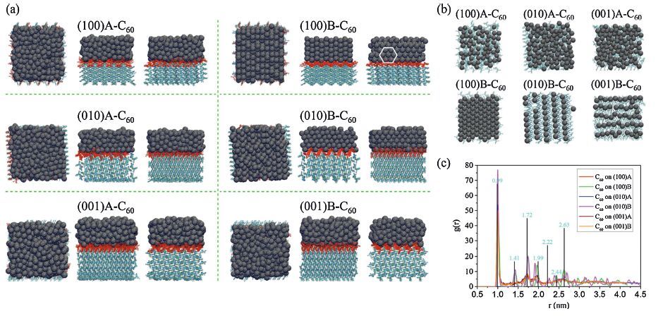
The surface stability can be characterized by surface energy (Fig. 4b),which is also an important property that influences the possibility of interaction with other media and adhesiveness,and thus the molecular self-assembly dynamics. In the same normal,the estimated surface enegies for A surfaces are higher than those for B surfaces,which is consistent with the bigger changes in the A surfaces under thermalization. The calculated adhesion energies of the topmost molecules for the A surfaces are relatively weaker than their counterparts for the B surfaces,confirming the surface energy results. These are consistent with the surface stacking compactness (lossely stacked A surfaces vs. B surfaces in a tight pp stacking). As expected,the loose and unstable A surfaces facilitate intermixing among the DTDCTB and C60 molecules. In particular,for the most unstable and disordered (0 1 0)A and (0 0 1)A surfaces,the growing C60 molecules first settle into the ‘holes’ surrounded by mobile DTDCTB molecules and then go deeper into the holes,and finally push the DTDCTB molecules upward into the C60 layers (Fig. 6a,b). This ‘burrowing’ picture has been also observed recently for C60 on pentacene(0 1 0) by Clancy et al . and Brédas et al.
We now turn to the effect of surface landscape. As displayed in Figs. 3b,Figs. 4a and Figs. 4c,all the relatively ordered surfaces have furrows of different shapes and/or sizes. The (1 0 0)A and (0 0 1)B surfaces possess rectangle-like furrows with similar depths of 0.6∼0.7 nm but quite different widths of ca. 0.7 and 1.7 nm,respectively. The furrow width of the (1 0 0)A surface is too small to contain C60 freely,because of the van der Waals diameter of C60 of around 1.0 nm,as a result,the early deposited C60 will dig and squeeze into the furrows randomly,leading to disorder and intermixing at the interface. On the contrary,the quite large furrow width for the (0 0 1)B surface results in the early deposited C60 molecules always moving back and forth between the furrow walls,facilitating disordered packing for the later deposited C60 molecules. Interesting to us is funnel-like furrows on the (1 0 0)B and (0 1 0)B surfaces,which can leave C60 molecules stay steadily in the furrow valley,due to enough furrow widths for both surfaces (1.7∼1.8 nm). While different furrow depths between the two surfaces bring about different packing modes. For the (0 1 0)B surface,the first layer of C60 molecules exactly fill in the furrows (∼1.2 nm in depth),rendering the surface relatively smooth and stable. As a consequence,the following C60 molecules are arranged in an ordered and layered structure. For the (1 0 0)B surface,the flattened furrows (∼0.5 nm in depth) with the matched pattern and excellent stability induce an ordered face-centered cubic packing for C60 with the hexagonal close packing (hcp) mode.
Except the surface stability,ordering and landscape,it is seen that the phenyl groups of the topmost layer of DTDCTB are hidden underneath for the (1 0 0)B surface or restrained by adjacent molecular groups for the (0 1 0)B surface. This also benefits the formation of an ordered C60 packing. In contrast,the phenyl groups are exposed to vacuum for the (1 0 0)A and (0 0 1)B surfaces and rotate dynamically due to lack of steric effects,which is also responsible for the irregular C60 packing.
In summary,the MD simulations clearly demonstrate the interfacial and thin-film morphologies strongly depend on the integrated impact of surface stability,ordering,landscape,and molecular orientation. In particular,C60 crystallization only appear on the surface that presents high ordering,good stability,matched landscape and restricted motion for the exposed molecular groups,such as the (1 0 0)B and (0 1 0)B surfaces,otherwise both the interfacial and bulk packing structures will become amorphous.
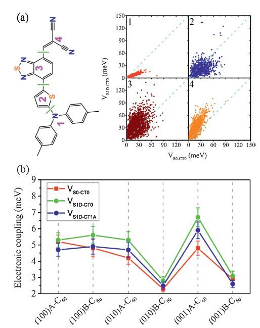
In addition,the competition between ED and CR in the closest DTDCTB/C60 complexes derived from the MD simulated interfaces were examined by computing the ED couplings (VS1D-CT0) and the CR couplings (VS0-CT0) using the method introduced in Section 2. There are five main findings: (1) When C60 moves from the electron-donating unit to the electron-withdrawing unit of DTDCTB,VS1D-CT0 becomes more competitive relative to VS0-CT0 (Fig. 7a). (2) Exposure of side nonconjugated groups,i.e .,phenyl in DTDCTB,will reduce electronic couplings. For the (0 1 0)B-C60 and (0 0 1)B-C60 interfaces,the average couplings are thus quite small (Fig. 7b). (3) The most stable surface for DTDCTB,i.e. (1 0 0)B leads to strong couplings,which could be comparable to those in the intermixed interfaces. Furthermore,its crystalline fullerene packing can enable ultrafast charge separation,as mentioned above. (4) The ED couplings involved in the lowest excited CT state (VS1D-CT1A) show an average value similar to VS1D-CT0 for all the DTDCTB-C60 interfaces,suggesting that the hot CT states can play a critical role in ED,as emphasized in Section 2. (5) It is noted that the standard deviation of electronic couplings is very significant,even larger than the average value (Fig. 7b). Therefore,in order to estimate the excited-state electron-transfer rates more reliably,time-dependent dynamics approaches,such as mean field and surface hopping strategies,would be a good choice [75, 76].
3.3. Influence of solvent evaporation rate and thermal annealing on the molecular packing and charge transport in DPP(TBFu)2Recently,solution-processed small-molecule OSCs have achieved the PCEs over 9% for single-junction devices,but most of them with high PCEs rely heavily on extra treatments of their active layers [40],such as solvent additive processing (SAP),thermal annealing (TA),and solvent vapor annealing (SVA),to form a nanoscale interpentrating network of D and A phases with appropriate domain sizes (10-20 nm) and to optimize the local interfacial configurations for efficient charge generation. For example,a high boiling point additive can reduce the solvent evaporation rate and thus allow a longer time for molecular selfassembly during solution processing,finally leading to a higher degree of phase separation and a larger domain size. Such distinct nanostructural variations are deemed to be responsible for the improved OPV performance obtained by additional treatments or altering the film-processing conditions [40]. On the other hand,even with an ideal domain size,the molecular stacking and ordering can also play an important role in exciton diffusion/ dissociation and charge transport behaviors [77-82].

|
Download:
|
| Figure 7. (a) Comparisonbetweenthe coupling for charge recombinationfromthe lowest CT state (CT0) to the ground state (S0) (VS0-CT0) and the coupling for dissociation of the lowest singlet exicited state on DTDCTB (S1D) into CT0 (VS1D-CT0) for the DTDCTB/C60 complexes extracted fromthe (0 1 0)A-C60 interface as a functionof the intermolecular arrangements [a complex in which the C60 is closest to the center of mass of fragment 1 (or 2,3,4) ofDTDCTB (consideredwithin 4Å ),belongs to configuration 1 (or 2,3,4)]; (b) Averages of VS0-CT0,VS1D-CT0 and VS1D-CT1A [the coupling for dissociation of S1D into the lowest excited CT state (CT1A,that arises fromthe first excitation of C60 anion)] for all the DTDCTB-C60 interfaces (the standard deviation is scaled by a factor of 0.05 for convenient display). Adapted from Han et al. [24]. | |
It is well known that the high and balanced carrier mobilities in OSCs can mitigate nongeminate CR and thus give rise to a significant increase in the device fill factor (FF) [83-85]. By analyzing the mobilities and FFs of a variety of solution-processed small-molecule OSCs,Nguyen et al. suggested that hole and electron mobilities should be larger than 10-4 cm2/Vs to obtain high FFs (>65%) [85]. Very often,hole mobilities are relatively low and less than 10-4 cm2/Vs in OSCs. Generally,neat film hole mobility for a given molecule determines the upper limit of blend film hole mobilities,thus neat film mobilty measurements can be used to screen potential small-molecule donor materials. Here,we are particularly interested in probing the dependence of the local molecular packing and hole mobilities of neat donor films on processing conditions. In the below,we analyze the effect of solvent evaporation rate (which is dependent on the solvent natures and the presence of additives) and TA on the local molecular packing and ordering of a pure DPP(TBFu)2 donor material. DPP(TBFu)2,as a prototype small-molecule donor,has been widely investigated experimentally [52-55],the annealed DPP(TBFu)2/PC71BM blend films yielded relatively high PCEs of up to 4.4% in 2009 [52]. Ordered crystalline regions of DPP(TBFu)2 were induced by SVA or TA in the blend,which is regarded as the driving force for phase separation [53, 54]. Furthermore,the correlation between molecular stacking and hole mobility is revealed through a multi-scale modeling that combines electronicstructure calculations,electrical network analysis,and kinetic Monte Carlo (KMC) simulation [59-63, 71, 80, 86-88].
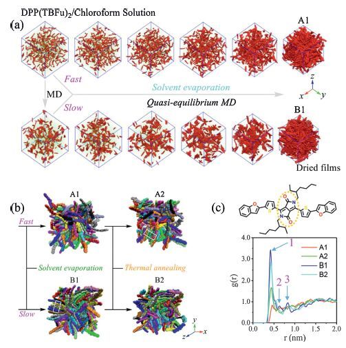
Firstly,the modeling schemes of solvent evaporation process and TA treatment are presented. Here,a solution with 400 DPP(TBFu)2 and 50000 chloroform molecules was constructed (with a balanced box size of nearly 20 nm in three dimensions),shown in Fig. 8a,then,a quasi-equilibrium molecular dynamics approach with NPT sensemble (P = 1 bar,T = 300 K) were employed by randomly removing 100 solvent molecules from the solution in every predefined time dt to mimic the solvent evaporation process. The evaporation rate was controlled by varying the dt: 1 ps (fast) and 100 ps (slow). The evolution of solutions with fast and slow rate is also exhibited in Fig. 8a and the resultant thin films are respectively labeled as A1 and B1. Using this scheme,Pao et al. have investigated the evolution of the nanomorphologies of P3HT/PCBM blends during solution processing using coarse-grained MD simulations [74]. After solvent evaporation,the two dried samples were further equilibrated for 10 ns at 300 K. The TA treatment is as follows: the as-cast sample is firstly heated at 500 K for 10 ns,then quenched to 300 K,and eventually,equilibrated at 300 K for 10 ns. As a result,two annealed samples (A2 and B2,Fig. 8b) were obtained with respect to A1 and B1,respectively. The final balanced box sizes for all samples are about 7.5 nm in three dimensions.

|
Download:
|
| Figure 8. (a) Construction of a DPP(TBFu)2/chloroform solution and simulations of the supramolecular self-assemblies of DPP(TBFu)2 during solvent evaporation. The inherent alkyl chains of DPP(TBFu)2 and hydrogen atoms are neglected for visualizing the packing of conjugated backbones,and the chloroform molecules are simplified as points with the carbon atoms’ positions. DPP(TBFu)2 backbones and chloroform points are colored in red and green,respectively. The dried films obtained with relatively fast and slow evaporation rate are labeled as A1 and B1. (b) Molecular packing morphologies of as-cast (A1 and B1) and thermally annealed (A2 and B2) DPP(TBFu)2 thin films fabricated at a fast (A1 and A2) or slow (B1 and B2) solvent evaporation rate. The molecules are shown in distinct colors and the inherent alkyl chains and hydrogen atoms are omitted for highlighting the packing of conjugated backbones. (c) Center-of-mass radial distribution functions of the DPP moiety. Adapted from Han et al. [51]. | |
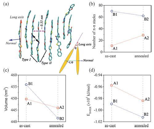
Apparently,the four well-fabricated samples have quite different bulk stacking nature (Fig. 8a,b),which are also quantified by the DPP COM RDFs (Fig. 8c). The first peaks are located at ∼0.4-0.5 nm,corresponding to a slip π-π stacking,thus their peak strengths can indicate the degree of crystallization. The corresponding number of π-π stacks for each sample was also evaluated to characterize the local orders. The fairly weak RDF peak at ∼0.46 nm for A1 indicates an almost amorphous packing. In stark contrast,there exist lots of well-organized domains in B1,confirmed by the very sharp first peak at ∼0.42 nm (slightly slip π-π stacks,type I in Fig. 9a),the distinct second peak at ∼0.64 nm (moderately slip π-π stacks,type II) and the third peak at ∼0.83 nm (about twice the first peak position). The number of π-π stacks for B1 (70) is nearly seven times that for A1 (11) (Fig. 9b). It is easy to understand that in the case of slower drying (the preparation process of B1),DPP(TBFu)2 molecules have enough time to reorient or self-organize to gain higher crystallinity. In fact,as a low boiling point solvent (only 61.2 ℃),without SAP,chloroform would lead to a very fast evaporation rate and thus a low crystallinity of the active layer. On the other hand,TA can allow recrystallization or reorientation in the active layer induced by thermal dynamic motions. The first RDF peak for A1 becomes much stronger and the peak intensity is almost double after TA (Fig. 8d). Also,the number of π-π stacks is increased from 11 to 29 (Fig. 9b). Indeed,some partially ordered regions appear in A2 (Fig. 8c). The results are consistent with previous experimental observations that the neat DPP(TBFu)2 films directly spin-casted from chloroform showed no sign of crystallinity and underwent crystallization upon TA. Surprisingly,to some extent,the degree of molecular packing order for the slow dried B1 is damaged after TA (Fig. 9b),which is ascribed from many voids in the as-cast sample.

|
Download:
|
| Figure 9. (a) An example snapshot of the well-ordered region from B1. A π-π stacking pair can be determined according to the distance between DPP COMs ( <0.5 nm) and two angles,i.e. the angle u between the long axes of the conjugated backbones and the angle w between the normal of the DPP planes (insert). Here,it can be regarded as a π-π stack when the pair exhibits u and w less than 158,considering the thermal dynamic motions and twisted molecular conformations. (b) Number of π-π stacks,(c) volume,and (d) intermolecular interaction energy (EINTER) for each sample. Adapted from Han et al. [51]. | |
Another key finding is that both the as-cast samples become more compact after TA,especially for B1. It is seen that many crystalline and relatively ‘rigid’ aggregates take shape during solution processing of B1,which will flock together after the solvents disappear,but leave considerable gaps among them. The percentage of the voids in the bulk volume of B1 is about 3.25% according to the relative change in volume for B1 to B2. We conclude that these voids will be squeezed by modulating the orientations and conformations of the boundary molecules during TA,however,such modulation is detrimental to the ‘pristine’ ordering. In contrast,the molecules in A1 are amorphous and more flexible,which are beneficial to the formation of a close packing. Therefore,TA enables the molecules to form more ordered π-π stacking. The driving forces for molecular reorganization or recrystallization upon TA,i.e. the intermolecular interaction (Fig. 9d) and thermal motion,have also been illuminated. Our conclusions are that,during TA,the driving force of recrystallization for A1 is mainly from strong π-π stacking interaction,while thermal motion to compress the inter-aggregate voids is responsible for the crystallinity reduction for B1.
A high FF depends on the efficient mesoscopic (10-20 nm) charge transport in pure D or A phase after CS. Recently,a graph methodology (or network theory) in combining with electronicstructure calculations was developed by Savoie et al. [80] to describe the mesoscopic electrical connectivity and charge percolation behaviors in organic semiconductors. To identify the ability of DPP(TBFu)2 molecules to create connected mesoscopic electrical networks for the four fabricated samples,we define an effective connection between molecules when the HOMO energy difference is smaller than 0.3 eV and electronic coupling is larger than a given threshold value. Electronic coupling (or transfer integral) between frontier molecular orbitals is one of critical parameters to determine the charge transport process between molecules. In the framework of network theory,given a certain value of electronic coupling threshold,fewer networks imply better electrical connectivity across the bulk material. At a large coupling threshold (≥ 10 meV),the number of networks is decreased with the increasing ordering of molecular packing among the four samples (Fig. 10a,c). It should be mentioned that a continuous and robust network can be formed only when each molecule has ≥ 2 connected neighbors. Therefore,the two as-cast samples and their annealed samples have similar capabilities to form effective mesoscopic electrical networks throughout the bulk volume,(Fig. 10b,d) which is due to the delocalized HOMOover the whole backbone of DPP(TBFu)2 providing efficient intermolecular electrical contacts. As a consequence,all the samples exhibit quite high hole mobilities of the same order of magnitude. Note that,the mobilities of the samples are estimated within the hopping description based on the semi-classical Marcus theory and a KMC simulation. Here,three forms of the square of the transfer integral,i.e.

|
Download:
|
| Figure 10. (a) Average number of networks (NNET); (b) Average number of molecules of the largest network (νMAX) as a function of electronic coupling threshold (VT) [the insets show the returned largest networks in an example snapshot of B1 at VT = 1,10,and 20 meV]; (c) Illustration of networks for a selected snapshot at VT = 5 and 10 meV [distinct electrical networks have a unique color and the total number of networks is specified] for each fabricated DPP(TBFu)2 sample. (a) Average number of connections per molecule (NC) in DPP(TBFu)2 samples as a function of electronic coupling threshold (VT); (b) Mass densities (ρ) and hole mobilities (μ) for each sample based on the charge-transfer rates estimated using <V>2, (<V>+R)2, and <V2>=<V2>+σ2 as the square of electronic couplings,respectively. Adapted from Han et al. [51]. | |
4. Conclusions
In this short review,we have summarized our recent works on theoretical simulation of molecular packing morphology and electronic processes in the active layers for organic solar cells. (1) The effect of interfacial intermolecular arrangements on excitondissociation and charge recombination was revealed by quantumchemical studies based on model and molecular dynamics simulated donor/acceptor complexes. In particular,the dominant role of hot charge-transfer states in the exciton-dissociation process is highlighted. (2) The impact of donor surfaces with different features on fullerene packing and interfacial morphologies was analyzed by atomistic simulations. It was pointed out that interfacial intermixing and fullerene crystallization rely heavily on a combinational role of surface stability,landscape,and molecular orientation. (3) The molecular packing and ordering of a neat small-molecule donor material were investigated through atomistic simulations as a function of solvent evaporation rate and thermal annealing. Furthermore,the correlation between the resultant packing morphologies and the charge transport behaviors was revealed. These works could provide an unparalleled insight into molecular packing configurations in the ‘buried’ active layers and are helpful to obtain reliable structure-property relationships.
Acknowledgment We are very grateful to the financial support from the National Natural Science Foundation of China ( No . 91333117),the National Basic Research (973) Program of the Ministry of Science and Technology of China ( No . 2014CB643506),and the Strategic Priority Research Program of the Chinese Academy of Sciences (No. XDB12020200).| [1] | S.R. Forrest. The path to ubiquitous and low-cost organic electronic appliances on plastic. Nature 428 (2004) 911–918. |
| [2] | B. Kippelen, J.L. Brédas. Organic photovoltaics. Energy Environ. Sci. 2 (2009) 251–261. |
| [3] | G. Li, R. Zhu, Y. Yang. Polymer solar cells. Nat. Photon. 6 (2012) 153–161. |
| [4] | A. Mishra, P. Bäuerle. Small molecule organic semiconductors on the move: promises for future solar energy technology. Angew. Chem. Int. Ed. 51 (2012) 2020–2067. |
| [5] | P. Kumar, S. Chand. Recent progress and future aspects of organic solar cells. Prog. Photovolt. Res. Appl. 20 (2012) 377–415. |
| [6] | Y.W. Su, S.C. Lan, K.H. Wei. Organic photovoltaics. Mater. Today 15 (2012) 554–562. |
| [7] | S.B. Darling, F.Q. You. The case for organic photovoltaics. RSC Adv. 3 (2013) 17633–17648. |
| [8] | L.Y. Lu, T.Y. Zheng, Q.H. Wu, et al. Recent advances in bulk heterojunction polymer solar cells. Chem. Rev. 115 (2015) 12666–12731. |
| [9] | J.D. Chen, C.H. Cui, Y.Q. Li, et al. Single-junction polymer solar cells exceeding 10% power conversion efficiency. Adv. Mater. 27 (2015) 1035–1041. |
| [10] | Q. Zhang, B. Kan, F. Liu, et al. Small-molecule solar cells with efficiency over 9%. Nat. Photon. 9 (2015) 35–41. |
| [11] | B. Kan, Q. Zhang, M.M. Li, et al. Solution-processed organic solar cells based on dialkylthiol-substituted benzodithiophene unit with efficiency near 10%. J. Am. Chem. Soc. 136 (2014) 15529–15532. |
| [12] | B. Kan, M.M. Li, Q. Zhang, et al. A series of simple oligomer-like small molecules based on oligothiophenes for solution-processed solar cells with high efficiency. J. Am. Chem. Soc. 137 (2015) 3886–3893. |
| [13] | K. Sun, Z.Y. Xiao, S.R. Lu, et al. A molecular nematic liquid crystalline material for high-performance organic photovoltaics. Nat. Commun 6 (2015) 6013. |
| [14] | C.H. Cui, X. Guo, J. Min, et al. High-performance organic solar cells based on a small molecule with alkylthio-thienyl-conjugated side chains without extra treatments. Adv. Mater. 27 (2015) 7469–7475. |
| [15] | J.L. Brédas, J.E. Norton, J. Cornil, V. Coropceanu. Molecular understanding of organic solar cells: The challenges. Acc. Chem. Res. 42 (2009) 1691–1699. |
| [16] | T.M. Clarke, J.R. Durrant. Charge photogeneration in organic solar cells. Chem. Rev. 110 (2010) 6736–6767. |
| [17] | Y.P. Yi, V. Coropceanu, J.L. Brédas. Exciton-dissociation and charge-recombination processes in pentacene/C60 solar cells: Theoretical insight into the impact of interface geometry. J. Am. Chem. Soc. 131 (2009) 15777–15783. |
| [18] | D. Beljonne, J. Cornil, L. Muccioli, et al. Electronic processes at organic organic interfaces: insight from modeling and implications for opto-electronic devices. Chem. Mater. 23 (2010) 591–609. |
| [19] | A. Ojala, A. Petersen, A. Fuchs, et al. Merocyanine/C60 planar heterojunction solar cells: effect of dye orientation on exciton dissociation and solar cell performance. Adv. Funct. Mater. 22 (2012) 86–96. |
| [20] | B.P. Rand, D. Cheyns, K. Vasseur, et al. The impact of molecular orientation on the photovoltaic properties of a phthalocyanine/fullerene heterojunction. Adv. Funct. Mater. 22 (2012) 2987–2995. |
| [21] | Z. Guo, D.Y. Lee, R.D. Schaller, et al. Relationship between interchain interaction, exciton delocalization, and charge separation in low-bandgap copolymer blends. J. Am. Chem. Soc. 136 (2014) 10024–10032. |
| [22] | H. Tamura, I. Burghardt. Ultrafast charge separation in organic photovoltaics enhanced by charge delocalization and vibronically hot exciton dissociation. J. Am. Chem. Soc. 135 (2013) 16364–16367. |
| [23] | X.X. Shen, G.C. Han, D. Fan, Y.J. Xie, Y.P. Yi. Hot charge-transfer states determine exciton dissociation in the DTDCTB/C60 complex for organic solar cells: a theoretical insight. J. Phys. Chem. C 119 (2015) 11320–11326. |
| [24] | G.C. Han, X.X. Shen, Y.P. Yi. Deposition growth and morphologies of C60 on DTDCTB surfaces: An atomistic insight into the integrated impact of surface stability, landscape, and molecular orientation. Adv. Mater. Interfaces 2 (2015) 1500329. |
| [25] | A.E. Jailaubekov, A.P. Willard, J.R. Tritsch, et al. Hot charge-transfer excitons set the time limit for charge separation at donor/acceptor interfaces in organic photovoltaics. Nat. Mater. 12 (2013) 66–73. |
| [26] | G. Grancini, D. Polli, D. Fazzi, et al. Transient absorption imaging of P3HT:PCBM photovoltaic blend: evidence for interfacial charge transfer state. J. Phys. Chem. Lett. 2 (2011) 1099–1105. |
| [27] | H. Ohkita, S. Cook, Y. Astuti, et al. Charge carrier formation in polythiophene/ fullerene blend films studied by transient absorption spectroscopy. J. Am. Chem. Soc. 130 (2008) 3030–3042. |
| [28] | L.Y. Lin, Y.H. Chen, Z.Y. Huang, et al. A low-energy-gap organic dye for highperformance small-molecule organic solar cells. J. Am. Chem. Soc. 133 (2011) 15822–15825. |
| [29] | Y.H. Chen, L.Y. Lin, C.W. Lu, et al. Vacuum-deposited small-molecule organic solar cells with high power conversion efficiencies by judicious molecular design and device optimization. J. Am. Chem. Soc. 134 (2012) 13616–13623. |
| [30] | X.Z. Che, X. Xiao, J.D. Zimmerman, D.J. Fan, S.R. Forrest. High-efficiency, vacuumdeposited, small-molecule organic tandem and triple-junction photovoltaic cells. Adv.[31_TD$DIF]Energy Mater. 4 (2014) 1400568. |
| [31] | H.W. Lin, Y.H. Chen, Z.Y. Huang, et al. Highly efficient bifacial transparent organic solar cells with power conversion efficiency greater than 3% and transparency of 50%. Org. Electron. 13 (2012) 1722–1728. |
| [32] | H.W. Lin, H.W. Kang, Z.Y. Huang, et al. An effective bilayer cathode buffer for highly efficient small molecule organic solar cells. Org. Electron. 13 (2012) 1925–1929. |
| [33] | H.W. Lin, C.W. Lu, L.Y. Lin, et al. Pyridine-based electron transporting materials for highly efficient organic solar cells. J. Mater. Chem. A 1 (2013) 1770–1777. |
| [34] | A.Y. Chang, Y.H. Chen, H.W. Lin, et al. Charge carrier dynamics of vapor-deposited small-molecule/fullerene organic solar cells. J. Am. Chem. Soc. 135 (2013) 8790–8793. |
| [35] | D. Cheyns, M. Kim, B. Verreet, B.P. Rand. Accurate spectral response measurements of a complementary absorbing organic tandem cell with fill factor exceeding the subcells. Appl. Phys. Lett. 104 (2014) 093302. |
| [36] | L. Ye, H.H. Xu, H. Yu, et al. Ternary bulk heterojunction photovoltaic cells composed of small molecule donor additive as cascade material. J. Phys. Chem. C 118 (2014) 20094–20099. |
| [37] | S. Nunomura, X.Z. Che, S.R. Forrest. Charge trapping in mixed organic donor-acceptor semiconductor thin films. Adv. Mater. 26 (2014) 7555–7560. |
| [38] | H.S. Shim, F. Lin, J. Kim, et al. Efficient vacuum-deposited tandem organic solar cells with fill factors higher than single-junction subcells. Adv.[31_TD$DIF]Energy Mater. 5 (2015) 1500228. |
| [39] | O.L. Griffith, X.Liu, J.A. Amonoo, etal.. Charge transport and excitondissociation in organic solar cells consisting of dipolar donors mixed with C70. Phys. Rev. B 92 (2015) 085404. |
| [40] | Y. Huang, E.J. Kramer, A.J. Heeger, G.C. Bazan. Bulk heterojunction solar cells: morphology and performance relationships. Chem. Rev. 114 (2014) 7006–7043. |
| [41] | Y. Zhou, T. Taima, T. Kuwabara, K. Takahashi. Efficient small-molecule photovoltaic cells using a crystalline diindenoperylene film as a nanostructured template. Adv. Mater. 25 (2013) 6069–6075. |
| [42] | J.D. Zimmerman, X. Xiao, C.K. Renshaw, et al. Independent control of bulk and interfacial morphologies of small molecular weight organic heterojunction solar cells. Nano Lett. 12 (2012) 4366–4371. |
| [43] | B. Song, C. Rolin, J.D. Zimmerman, S.R. Forrest. Effect of mixed layer crystallinity on the performance of mixed heterojunction organic photovoltaic cells. Adv. Mater. 26 (2014) 2914–2918. |
| [44] | N.C. Miller, E. Cho, M.J.N. Junk, et al. Use of X-ray diffraction, molecular simulations, and spectroscopy to determine the molecular packing in a polymerfullerene bimolecular crystal. Adv. Mater. 24 (2012) 6071–6079. |
| [45] | L. Muccioli, G. D'Avino, C. Zannoni. Simulation of vapor-phase deposition and growth of a pentacene thin film on C60(001). Adv. Mater. 23 (2011) 4532–4536. |
| [46] | G. D'Avino, L. Muccioli, C. Zannoni. From chiral islands to smectic layers: a computational journey across sexithiophene morphologies on C60. Adv. Funct. Mater. 25 (2015) 1985–1995. |
| [47] | R.A. Cantrell, C. James, P. Clancy. Computationally derived rules for persistence of C60 nanowires on recumbent pentacene bilayers. Langmuir 27 (2011) 9944–9954. |
| [48] | Y.T. Fu, C. Risko, J.L. Brédas. Intermixing at the pentacene-fullerene bilayer interface: a molecular dynamics study. Adv. Mater. 25 (2013) 878–882. |
| [49] | Y.T. Fu, D.A. da Silva Filho, G. Sini, et al. Structure and disorder in squaraine-C60 organic solar cells: a theoretical description of molecular packing and electronic coupling at the donor-acceptor interface. Adv. Funct. Mater. 24 (2014) 3790–3798. |
| [50] | T. Liu, D.L. Cheung, A. Troisi. Structural variability and dynamics of the P3HT/ PCBM interface and its effects on the electronic structure and the charge-transfer rates in solar cells. Phys. Chem. Chem. Phys. 13 (2011) 21461–21470. |
| [51] | G.C. Han, X.X. Shen, R.H. Duan, H. Geng, Y.P. Yi. Revealing the influence of the solvent evaporation rate and thermal annealing on the molecular packing and charge transport of DPP(TBFu)2. J. Mater. Chem. C . DOI:10.1039/C6TC01201A |
| [52] | B. Walker, A.B. Tamayo, X.D. Dang, et al. Nanoscale phase separation and high photovoltaic efficiency in solution-processed, small-molecule bulk heterojunction solar cells. Adv. Funct. Mater. 19 (2009) 3063–3069. |
| [53] | A. Viterisi, F. Gispert-Guirado, J.W. Ryan, E. Palomares. Formation of highly crystalline and texturized donor domains in DPP(TBFu)2:PC71BM SM-BHJ devices via solvent vapour annealing: implications for device function. J. Mater. Chem. 22 (2012) 15175–15182. |
| [54] | A. Sharenko, M. Kuik, M.F. Toney, T.Q. Nguyen. Crystallization-induced phase separation in solution-processed small molecule bulk heterojunction organic solar cells. Adv. Funct. Mater. 24 (2014) 3543–3550. |
| [55] | J.H. Liu, Y. Zhang, H. Phan, et al. Effects of stereoisomerism on the crystallization behavior and optoelectrical properties of conjugated molecules. Adv. Mater. 25 (2013) 3645–3650. |
| [56] | E.F. Valeev, V. Coropceanu, D.A. da Silva Filho, S. Salman, J.L. Bredas. Effect of electronic polarization on charge-transport parameters in molecular organic semiconductors. J. Am. Chem. Soc. 128 (2006) 9882–9886. |
| [57] | A.A. Voityuk, N. Rösch. Fragment charge difference method for estimating donoracceptor electronic coupling: application to DNA[32_TD$DIF]pi-stacks. J. Chem. Phys. 117 (2002) 5607–5616. |
| [58] | R.J. Cave, M.D. Newton. Generalization of the Mulliken-Hush treatment for the calcualtion of electron transfer matrix elements. Chem. Phys. Lett. 249 (1996) 15–19. |
| [59] | Q. Wu, T. Van Voorhis. Direct optimization method to study constrained systems within density-functional theory. Phys. Rev. A 72 (2005) 024502. |
| [60] | J. Ridley, M. Zerner. An intermediate neglect of differential overlap technique for spectroscopy: pyrrole and the azines. Theor. Chim. Acta 32 (1973) 111–134. |
| [61] | K. Nishimoto, N. Mataga. Electronic structure and spectra of some nitrogen heterocycles. Z. Phys. Chem. 12 (1957) 335–338. |
| [62] | N. Mataga, K. Nishimoto. Electronic structure and spectra of nitrogen heterocycles. Z. Phys. Chem. 13 (1957) 140–157. |
| [63] | R.A. Marcus. Electron transfer reactions in chemistry. Theory and experiment. Rev. Mod. Phys. 65 (1993) 599–610. |
| [64] | G.J. Nan, X.D. Yang, L.J. Wang, Z.G. Shuai, Y. Zhao. Nuclear tunneling effects of charge transport in rubrene, tetracene, and pentacene. Phys. Rev. B 79 (2009) 115203. |
| [65] | S.W. Yin, L.L. Li, Y.M. Yang, J.R. Reimers. Challenges for the accurate simulation of anisotropic charge mobilities through organic molecular crystals: the (phase of mer-Tris (8-hydroxyquinolinato)aluminum(III) (Alq3) crystal. J. Phys. Chem. C 116 (2012) 14826–14836. |
| [66] | M.H. Lee, B.D. Dunietz, E. Geva. Calculation from first principles of intramolecular golden-rule rate constants for photo-induced electron transfer in molecular donor-acceptor systems. J. Phys. Chem. C 117 (2013) 23391–23401. |
| [67] | J. Jortner. Temperature dependent activation energy for electron transfer between biological molecules. J. Chem. Phys. 64 (1976) 4860–4867. |
| [68] | A. Nitzan, J. Jortner. Effects of vibrational relaxation on molecular electronic transitions. J. Chem. Phys. 58 (1973) 2412–2434. |
| [69] | A. Warshel, M. Levitt. Theoretical studies of enzymic reactions: dielectric, electrostatic and steric stabilization of the carbonium ion in the reaction of lysozyme. J. Mol. Biol. 103 (1976) 227–249. |
| [70] | T. Liu, A. Troisi. Absolute rate of charge separation and recombination in a molecular model of the P3HT/PCBM interface. J. Phys. Chem. C 115 (2011) 2406–2415. |
| [71] | S. Di Motta, E. Di Donato, F. Negri, et al. Resistive molecular memories: influence of molecular parameters on the electrical bistability. J. Am. Chem. Soc. 131 (2009) 6591–6598. |
| [72] | S. Grimme, J. Antony, S. Ehrlich, H. Krieg. A consistent and accurate ab initio parametrization of density functional dispersion correction (DFT-D) for the 94 elements H-Pu. J. Chem. Phys. 132 (2010) 154104. |
| [73] | I. Akimoto, M. Ashida, K. Kan'no. Luminescence from C60 single crystals in glassy phase under site-selective excitation. Chem. Phys. Lett. 292 (1998) 561–566. |
| [74] | C.K. Lee, C.W. Pao. Nanomorphology evolution of P3HT/PCBM blends during solution-processing from coarse-grained molecular simulations. J. Phys. Chem. C 118 (2014) 11224–11233. |
| [75] | L.J. Wang, O.V. Prezhdo, D. Beljonne. Mixed quantum-classical dynamics for charge transport in organics. Phys. Chem. Chem. Phys. 17 (2015) 12395–12406. |
| [76] | L.J. Wang, R. Long, O.V. Prezhdo. Time-domain ab initio modeling of photoinduced dynamics at nanoscale interfaces. Annu. Rev. Phys. Chem. 66 (2015) 549–579. |
| [77] | R.M. Pinto, E.M.S. Maçôas, A.I.S. Neves, et al. Effect of molecular stacking on exciton diffusion in crystalline organic semiconductors. J. Am. Chem. Soc. 137 (2015) 7104–7110. |
| [78] | V. Rühle, A. Lukyanov, F. May, et al. Microscopic simulations of charge transport in disordered organic semiconductors. J. Chem. Theory Comput. 7 (2011) 3335–3345. |
| [79] | M. Williams, N.R. Tummala, S.G. Aziz, C. Risko, J.L. Brédas. Influence of molecular shape on solid-state packing in disordered PC61BM and PC71BM fullerenes. J. Phys. Chem. Lett. 5 (2014) 3427–3433. |
| [80] | B.M. Savoie, K.L. Kohlstedt, N.E. Jackson, et al. Mesoscale molecular network formation inamorphousorganic materials. Proc.Natl.Acad. Sci 111 (2014) 10055–10060. |
| [81] | Z. Li, X. Zhang, Y. Zhang, et al. Hole transport in diketopyrrolopyrrole (DPP) small molecules: a joint theoretical and experimental study. J. Phys. Chem. C 117 (2013) 6730–6740. |
| [82] | V.D. Mihailetchi, J. Wildeman, P.W.M. Blom. Space-charge limited photocurrent. Phys. Rev. Lett. 94 (2005) 126602. |
| [83] | A. Baumann, J. Lorrmann, D. Rauh, C. Deibel, V. A new approach for probing the mobility and lifetime of photogenerated charge carriers in organic solar cells under real operating conditions,. Adv. Mater. 24 (2012) 4381–4386. |
| [84] | C.M. Proctor, J.A. Love, T.Q. Nguyen. Mobility guidelines for high fill factor solution-processed small molecule solar cells. Adv. Mater. 26 (2014) 5957–5961. |
| [85] | A.B. Tamayo, X.D. Dang, B. Walker, et al. A low band gap, solution processable oligothiophene with a dialkylated diketopyrrolopyrrole chromophore for use in bulk heterojunction solar cells. Appl. Phys. Lett. 94 (2009) 103301. |
| [86] | L.J. Wang, Q.K. Li, Z.G. Shuai, L.P. Chen, Q. Shi. Multiscale study of charge mobility of organic semiconductor with dynamic disorders. Phys. Chem. Chem. Phys. 12 (2010) 3309–3314. |
| [87] | L.J. Wang, G.J. Nan, X.D. Yang, et al. Computational methods for design of organic materials with high charge mobility. Chem. Soc. Rev. 39 (2010) 423–434. |
| [88] | S. Canola, F. Negri. Anisotropy of the n-type charge transport and thermal effects in crystals of a fluoro-alkylated naphthalene diimide: a computational investigation. Phys. Chem. Chem. Phys. 16 (2014) 21550–21558. |
| [89] | C.X. Zhao, S. Xiao, G. Xu. Density of organic thin films in organic photovoltaics. J. Appl. Phys. 118 (2015) 044510. |