 2016, Vol. 27


Organic semiconductors have aroused increasing attentions in recent years due to their outstanding performances and potential applications in electronic devices, such as organic field-effect transistors (OFETs) [1-6], organic solar cells [7], organic light- emitting diodes (OLEDs) [8]. These devices exhibit numerous advantages compared with inorganic semiconductor counterparts, including flexibility, low-cost and low-temperature processability [4, 9-11]. Of all those fabricated organic electronic devices, OFETs are critically fundamental components for integrated circuits, primarily act as switches and signal-processing elements for practical applications, like radio-frequency identification tags and active matrix displays [2, 3, 12]. Normally, device performances have extremely close relationships with crystalline structures and imperfections ofthe crystalline structures always account for poor performances [13, 14]. Imperfections such as grain boundaries and molecular disorders not only influence the quality of obtained crystalline morphologies, but also hinder the charge transport by scattering charge carriers. Therefore, single-crystal organic semiconductors, which perform excellent properties with the highest order as well as purity, lead to superior charge carrier mobility among organic electronic materials [15-18]. So far, many methods have been proposed to fabricate organic devices based on organic single crystals [19-21].
Despite of all the advantages above, the scale-up of organic single crystals for practical applications is still challenging since the growth orientation and location as well as alignment of single crystals are usually difficult to control. While large-scale industrial applications with high integration demand high uniformity and minimal cross-talk between neighboring devices [22], it is of extreme importance to pattern single crystals at well-designed locations. The development of patterning and alignment techniques is indispensable for the realization of integrated devices, and will undoubtedly facilitate the progress of single-crystal organic semiconductors for practical applications [23]. Over the last decade, many efforts have been devoted to promote various strategies for growing organic semiconductor molecules into well- aligned patterns as well as ordered arrays with the positions and locations under control, precisely. In this article, we review the recent progress of this research topic [24-36].
2. Crystal alignmentCharge carrier transport in organic single crystals has been demonstrated to be anisotropic [37-39]. Alignment of the crystals in a unidirectional fashion is, hence, necessary to achieve the potentially uniform OFET performance. Concentration and/or temperature gradients as well as tilted substrates have been used to control the crystallization direction [27, 29, 40-46]. Solutionshearing and droplet-pinned crystallization (DPC) method are two typical and facile approaches to align organic crystals.
As depicted in Fig. 1a, a solution of organic material was sandwiched between the heated device substrate, which can be modified to improve wetting, and the shearing substrate, which can be modified to cause dewetting. As the upper substrate moved steadily, the front of solution evaporated and created nuclei followed by additional organic molecules continuously flowing towards nuclei and self-organizing to form aligned structures. After solution-shearing, uniform crystalline film of quarterthio- phene (TMS-4T) were deposited parallel to the direction of the shearing movement and extended over the entire heated substrate (Fig. 1b) [47]. The shearing rate is a crucial parameter since fast shearing rates lead to very thin films and moderate crystalline structures. By optimizing the shearing speed, the conjugated backbones of 6, 13-bis(triisopropylsilylethynyl)pentacene (TIPS- pentacene) can be packed more tightly, resulting in reduced π-π stacking distance from 3.33 A to 3.08 A [48]. Since the introduced lattice strain within the crystal lattice effectively enlarged orbital overlap between component molecules, the charge carrier mobility of field-effect transistor increased from 0.8 cm2 V-1 s-1 to a higher one of 4.6 cm2 V-1 s-1 for unstrained and strained crystalline films, respectively. Meanwhile, solution concentration as well as substrate temperature also has a significant impact on crystalline film quality. Based on these observations, to optimize the performance of aligned organic single crystals, another two strategies were proposed based on solution-shearing. One is to combine solution-shearing method with wettability pattern of substrate [34]. Highly aligned TIPS-pentacene was found to preferentially grow on the wettable areas (Fig. 1d), with the substrate patterned with wetting/dewetting lines in advance (Fig. 1c). This method improved crystal textures and nucleation control by lateral confinement. The obtained TIPS-pentacene thin film, without significant grain boundaries, with the smallest pattern size of 0.5 μm exhibited an average mobility up to 2.7 cm2 V-1 s-1. The other is to modify the blade with micropillars to enhance mass transport. The crescent-shaped structures (Fig. 1e, f) induced recirculation behind the micropillars, so as to facilitate lateral mass transport. With enhanced fluid flow, the morphology of TIPS-pentacene thin film was remarkably enhanced (Fig. 1g) and the maximum mobility attained was as high as 11 cm2 V-1 s-1.

|
Download:
|
| Figure 1. (a) Schematic illustration of solution-shearing. (b) Bright-field optical microscopy (OM) image of prepared TMS-4T film,showing elongated crystalline structures. (c) Schematic illustration of substrate patterning and crystalline thin film growth by solution-shearing method. (d) Cross polarized optical microscopy (CPOM) image of solution- sheared TIPS-pentacene thin films with 0.5 μm patterned line width. The scale bar is 25 μm and the white arrow indicates the shearing direction. (e) Schematic illustration of solution-shearing using a crescent micropillar-modified blade. The arrow shows the shearing direction. (f) Scanning electron micrograph (SEM) of the micropillar-patterned blade. (g) CPOM image of TIPS-pentacne thin film with micropillars. Adapted from References [47] (© 2008 Wiley),[34] (© 2013 Wiley) and [35] (© 2013 Nature Publishing Group) with permission. | |
Based on solution shearing method, another approach named as rapid annealing self-solution-shearing (RASSS) was reported to accomplish quick creation of well-aligned organic single crystals of 9, 10-bis(phenylethynyl)anthracene (BPEA) in a large scale by controlling the receding direction of the contact line based on the surface tension model [49].
DPC is another useful method to obtain highly aligned organic single crystals. The small silicon wafer at the center of the substrate, termed as pinner, pins the droplet to avoid unstable sliding of solution and provides steady receding direction (Fig. 2a) [50]. During drying of the solution, nuclei formed first at the contact line and crystals grew along the receding direction. Once the solution was fully evaporated, crystal arrays pattern would be formed surrounding the pinner. DPC is easily scalable since the pinners can be patterned in a large area over the entire substrate to control the nucleation density with high crystallinity, as illustrated in Fig. 2b. Two parameters are essential in DPC method, a high nuclei density and a steady contact line receding. Using this method, highly aligned C60 single crystals (Fig. 2c, d) were prepared and the electron mobility was as high as 11 cm2 V-1 s-1 by optimizing the growth condition of crystals with various solvents and concentrations. The record-high electron mobility [51] was further raised to 13.3 cm2 V-1 s-1 by highly aligned 6, 13-bis(triisopropylsilylethynyl)-5, 7, 12, 14-tetraazapentacene (TIPS- TAP) [52] single crystals grown by DPC method after solvent residue was carefully reduced. Besides, ambipolar charge transport of TIPS-pentacene [53] single crystals grown from non-polar solvents was discovered, with Au as source and drain electrodes [54, 55], proving that the existence of polar solvent residues in crystals is detrimental to electron transportation [51]. Moreover, DPC method is applicable to a variety of organic semiconductors, including 7, 7, 8, 8-tetracyanoquinodimethane (TCNQ), C60, pery- lene, anthracene, tetracene, TIPS-pentacene, TIPS-TAP, and dike- topyrrolopyrroles (DPP) derivatives [56-59]. Also, DPC method has been used to prepare bilayered single crystals (Fig. 2e) that exhibit ambipolar transport, memory and photovoltaic functions [32, 60, 61].

|
Download:
|
| Figure 2. (a) Schematic illustration of the DPC method. (b) Elongation of pinner leading to unidirectional parallel single-crystal arrays. (c) OM image of well-aligned C60 ribbon crystals. (d) Transmission electron microscopy (TEM) image of a ribbon crystal with a faceted edge; (inset) selected area electron diffraction (SAED) pattern of C60 ribbon,indicating single crystallinity. (e) OM image of bilayered heterojunctions with C60 crystals formed on (3-pyrrolinium)(CdCl3) ribbons. Adapted from References [50] (© 2012 American Chemical Society) and [60] (© 2015 Wiley) with permission. | |
In addition to the continuous receding of the meniscus used in the above two methods, incontinuous receding was employed to align crystals [62, 63]. Also, crystals were aligned physically by external fields such as electric field [44].
3. Crystal patterningPatterning organic semiconductors is especially competent to minimize cross-talk between two adjacent devices [64]. Two typical approaches to achieve crystal patterning are described below.
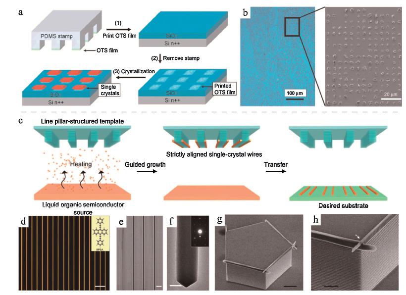
3.1. Selective nucleationThe higher surface energy associated with irregularities, such as step edges, indentions or protrusions, significantly decreases the barrier for heterogeneous nucleation, compared with that on a flatter surface [65]. Zhao and co-workers developed a method of alternating ridges and grooves on a silicon wafer by scouring the surface to create different energy domains for preferential nucleation and growth of 1, 5-diaminoanthraquinone (DAAQ) molecules [66]. However, scouring the substrate surface possesses a possible risk of damaging the substrate. In contrast, modifying the substrate with rough films is a more convenient way to create more uniformly specific energy domains and to acquire pattered crystalline structures. Bao and co-workers demonstrated a singlecrystal patterning process which is suitable for a wide range of organic semiconductor materials to fabricate large arrays of singlecrystal pattern directly onto source-drain electrodes [67, 68]. By microcontact printing process, octadecyltriethoxysilane (OTS) films were printed onto a SiO2/Si substrate, using a polydimethyl- siloxane (PDMS) stamp, into a desired pattern, and then crystal growth was realized by a vapor transport method (Fig. 3a). The substrate with OTS-stamped region exhibited a considerably larger degree of roughness compared with the SiO2 background, and acted as primary nucleation centers. Crystal nucleation of organic molecules such as pentacene, C60 and rubrene were restricted only to OTS-stamped region, rather than SiO2 background (Fig. 3b) [69]. OFETs based on rubrene single crystals patterned into a 14 × 14 transistor array exhibited mobility values ranging from 0.1 to 2.4 cm2 V-1 s-1. With the similar idea, Liu and coworkers utilized patterned single-walled carbon-nanotube (SWNT) bundles as templates to guide the crystallization of organic semiconductors, such as pentacene, tetracene and sexiphenylene, into singlecrystalline arrays [70]. SWNT bundles were transferred onto a cleaned SiO2/Si substrate by microcontact printing with a PDMS stamp. Organic crystals were subsequently vapor grown on the SWNT patterned regions. Since the surface of SWNT bundles is not flat and contains numerous surface steps, which provide favorable domains for crystal nucleation, the growth of crystals can be exactly restrained in these stamped sites and not observed on the pristine SiO2 background. Furthermore, pentacene and tetracene molecules were found crystallized on SWNT bundles with an edge- on orientation, which indicated the fact that these molecules underwent a rotation process into edge-on geometry through π-π interactions with SWNT bundles. Therefore, the strong (compared with the strength of interactions between molecules and the bare SiO2 substrate) π-π interactions between the aromatic organic molecules and the fully conjugated surface of SWNT bundles further amplify the effect of the rough morphology of the nanotubes, leading to highly preferential crystallization on SWNT bundles into a conformal fashion. OFETs based on arrays of pentacene single-crystal transistors performed typical mobilities ranging from 0.01 to 0.2 cm2 V-1 s-1, with the highest one of 0.4 cm2 V-1 s-1. Very recently, Wu and co-workers developed a guided physical vapor transport (GPVT) method to encourage favorable growth of organic single-crystal wires by using a pillar-structured substrate to guide the vapor flow (Fig. 3c) [71]. Because of the energy difference between the pillar top-walls and sidewalls, organic molecules tend to nucleate and grow along the pillar edges, producing long and highly aligned single-crystal wire arrays, which can be subsequently transferred to a desired substrate (Fig. 3d). Apart from regular linear arrangements (Fig. 3e, by tuning the pillar geometry, organic single-crystal wires can be joined with precisely controlled angles and positions (Fig. 3g, h).

|
Download:
|
| Figure 3. (a) Schematic procedure for growing organic single crystals on the substrate with PDMS-stamped OTS films by microcontact printing. (b) OM image of a large array of discrete pentacene single crystals grown on a OTS-patterned substrate; (right) SEM of the indicated area in the left image. (c) Schematic illustration of the GPVT method. (d) A dark-field fluorescent micrograph of BPEA crystals excited with a 325-nm ultraviolet irradiation; (inset) molecular structure of BPEA. (e) SEM of highly aligned BPEA wires. (f) TEM image of a single BPEA wire; (inset) SAED pattern indicating single-crystalline structure. (g) SEM of BPEA wire patterns on a pentagon-shaped micropillar. (h) Magnified image of (g),showing joined BPEA wires at the external angle structure of the micropillar. Scale bars,(d) 20 μm,(e) 5 μm,(f) 400 nm,(g) 10 μm,(h) 2 μm. Adapted from References [67] (© 2006 Nature Publishing Group) and [71] (© 2015 Nature Publishing Group) with permission. | |
3.2. Spatial confinement
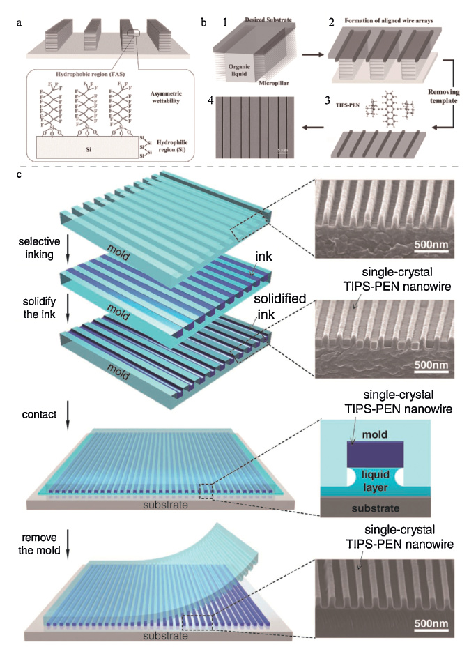
Confinement of the crystallization space in a patterned fashion results in patterned crystals. One of the convenient approaches is to confine the mother solutions for crystals in wettable areas surrounded by non-wettable regions [72-76]. For example, Wu and co-workers proposed an effective method, termed threedimensional dewetting mediated assembly (TDMA) to obtain single-crystal arrays by controlling the dewetting direction of organic semiconductor liquid, which was realized by the use of a line-pillar-structured template with different wettability patterns [77]. The line-pillar-structured template was fabricated through selective modification with a heptadecafluorodecyltrimethoxysi- lane (FAS) covered PDMS thin flat film by a hot pressing treatment to leave FAS molecules upon the pillar tops, leading to hydrophobicity, while sidewalls of the pillar, which was FAS-free, remained superhydrophilic (Fig. 4a). By introducing FAS molecules on the pillar tops, the difference of wettability of top-walls (hydrophobic) and sidewalls (hydrophilic) was able to split semiconductor liquid into regular liquid stripes as well as guide the unidirectional dewetting process of these regular liquid stripes. Once a solution of TIPS-pentacene was dropped onto the pillar- structured substrate, with a desired flat plastic substrate covered on the top, forming a "sandwich" assembly system, the capillary force generated by the gaps between micropillars together with the unidirectional force inside the liquid would guide the nucleation and crystallization process of organic molecules into well-aligned organic belts (Fig. 4b). After peeling off the desired flexible substrate from the silicon template, well-defined TIPS- pentacene with strict alignment was prepared (Fig. 4b-4) and OFETs based on these single-crystalline belts performed mobilities ranging from 4.68 to 11.31 cm2 V-1 s-1.

|
Download:
|
| Figure 4. (a) Schematic illustration of pillar-structured template with selectively modified micropillars with FAS-covered top and FAS-free sidewalls. (b) Schematic illustration of solution shrinkage process and formation of regular organic crystal belts (1-3) and SEM of strictly aligned single-crystalline TIPS-pentacene belt arrays (4) . (c) Procedure of single-crystal organic nanowire arrays fabrication. Adapted from References [77] (© 2016 Wiley) and [24] (© 2013 Wiley) with permission. | |
In addition, surface wettability pattern can be combined with inkjet printing [78], which is advantageous for minimizing material consumption. Before inkjet printing, the OTS covered surface of the channel regions was selectively exposed to deep ultraviolet (DUV) irradiation to provide controllable hydrophilic domains separated from hydrophobic surroundings [79]. Thus, the difference of surface energy directed the ink into the patterned hydrophilic area to cover the channel region. The confined ink led nucleation and growth to start from one end or both ends of the modified Au region, and finally resulted in the formation of a large crystal on the hydrophilic channel domain. The main advantage of this proposed technique is that by using inkjet printing, single crystals can be easily processed in large arrays with high-resolution spatial selectivity, as well as versatility in large area application. The inkjet printed TIPS-pentacene OFET arrays showed mobility as high as 0.6 cm2 V-1 s-1 (average of 0.2 cm2 V-1 s-1). Alternatively, crystallization space can be confined physically by splitting the mother solutions using templates [80-84]. For example, Jo and co-workers proposed another method based on spatial confinement combined with modified capillary force lithography (CFL) and successfully grew 2, 7-dioctyl[1]ben- zothieno[3, 2-b][1]benzothiophene (C8-BTBT) line pattern over a large area [85]. A prepatterned PDMS stamp (p-PDMS stamp) was conformally contacted with the droplets of C8-BTBT solution and spatially confined the solution in the trenches of the template. During the solidification process, capillary force drove the solution moving towards empty trenches and finally generated crystal lines in each PDMS trench after thermally annealing. By using this technique, the line-patterned crystals replicated exactly the dimensions of the p-PDMS stamp, with the width and the spacing simply duplicating the shape of the template above, while the height of the line pattern depends on the relationship between capillary and gravitational forces during the CFL process. Also, Park and co-workers reported a liquid-bridge-mediated nanotransfer molding (LB-nTM) method which enables simultaneous synthesis, alignment as well as controlled positioning of single-crystal organic semiconductor nanowires from molecular ink solutions [24]. As illustrated in Fig. 4c, by using a polyurethane acrylate (PUA) mold, self-assemblied and solidified organic molecules from the ink solution within the nano-channels of the mold formed single-crystal nanowires, which were next transferred to specific positions on a desired substrate. The polar solvent between the mold and the substrate formed a thin liquid layer, which generated a liquid bridge, i.e. capillary bridge, and as the liquid evaporated, the gradually increased capillary force attracted the two surface into contact and provided good conformal contact without any additional pressure to the mold. After drying, period arrays of single crystals formed on the desired positions after separation of the mold from the substrate. This direct printing method can also be used to fabricate multi-layer organic nanowires, and using this method, C60, poly(3-hexylthiophene) (P3HT), TIPS-pentacene single crystals were successfully manufactured in large arrays, with the best field-effect performance of OFET nanowire arrays based on TIPS-pentacene single crystals exhibited mobility as high as 1.52 cm2 V-1 s-1.
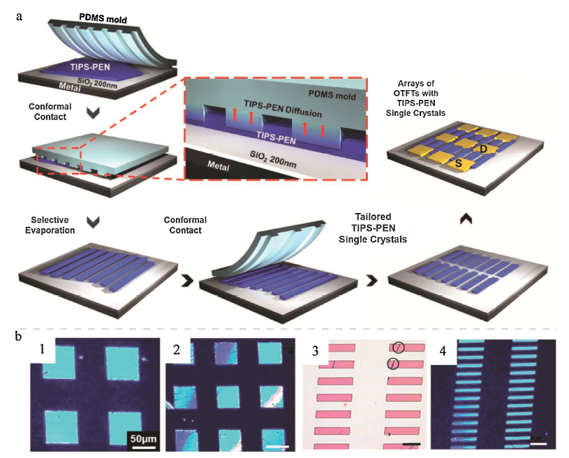
4. top-down methodApart from directly growing patterned and well-aligned organic crystals at desired locations on substrate, namely "bottom-up method", there is another effective and efficient way to create crystalline arrays which is termed as "top-down method". By dealing with pre-deposited organic crystals on a large range [86], the dimension as well as location of patterned arrays can be well controlled. Lee and co-workers developed a simple and facile method by abrupt heating of the substrate pre-deposited with amorphous rubrene films [87]. After abrupt heating under the optimum condition, crystalline rubrene films with highly ordered and uniaxially oriented single-crystalline grains were prepared and organic thin-film transistors (OTFTs) based on the high-quality crystalline rubrene films presented mobilities as high as 1.21 cm2 V-1 s-1. By combining abrupt heating method and a lift-off process, in situ patterning of crystalline rubrene films with high quality and accurate spatial resolution can be conveniently fabricated [88]. During the abrupt heating process, a PDMS stamp with prepatterned lines was pressed onto the rubrene film with an appropriate press and after detachment of the stamp, noncon- tacted rubrene films remained on the substrate, duplicating the pattern of the lift-off PDMS stamp. After this process, exquisite patterns of rubrene microwires composed of single-crystalline grains were achieved without any residue material remained on the SiO2 substrate and OFETs performed high mobility of 4.5 cm2 V-1 s-1. Another method termed as selective contact evaporation printing (SCEP) was proposed to fabricate singlecrystalline TIPS-pentacene by selectively etching a large and flat single-crystalline TIPS-pentacene film using a topographically prepatterned PDMS stamp (Fig. 5a) [89]. During the etching process, TIPS-pentacene molecules diffused into the PDMS mold, driven by the concentration gradient, which left no residual substances of crystals on the surface of PDMS mold, leading to tailored single-crystalline pattern of TIPS-pentacene arrays on the substrate. By designing the topography of the PDMS mold as well as the etching process, crystalline arrays of different shapes and dimensions can be practically obtained (Fig. 5b).

|
Download:
|
| Figure 5. (a) Schematic illustration of the SCEP process by using a PDMS mold with topographical line patterns,which is in conformal contact with the pre-deposited single-crystalline film,to tailor or etch the TIPS-pentacene film into desired fashion,followed subsequently by OTFT fabrication process. (b) OM images of patterned single-crystalline TIPS-pentacene by SCEP process with varied shapes and sizes of squares (1,2) and rectangles (3,4) . Adapted from Reference [89] with permission. © 2011 Wiley. | |
5. Conclusion
During the fast development of OFETs, more and more materials, especially in the single-crystalline form, emerge with excellent device performances. In order to further up scale the single-crystal OFETs for practical applications, alignment and patterning of the crystals are desired. Crystal alignment has been achieved mainly by solution methods where receding of meniscus is controlled. Crystal patterning typically relies on selective nucleation and/or spatial confinement of the crystallization. Despite all these achievements, novel design and further improvement of the crystallization methods are still needed to well accommodate the flexible/stretchable device configurations as well as the large-scale device processing. As more and more novel and practical crystallization approaches keep emerging, the future for the field of organic electronics based on single crystals is ever bright and we hope that the important recent progresses outlined herein will further inspire exquisite as well as effective techniques for large-area applications.
Acknowledgments This work was supported by the 973 Program (No. 2014CB643503), National Natural Science Foundation of China (Nos. 51373150, 51461165301), and Zhejiang Province Natural Science Foundation (No. LZ13E030002).| [1] | A. Tsumura, H. Koezuka, T. Ando. Macromolecular electronic device: field-effect transistor with a polythiophene thin film. Appl. Phys. Lett. 49 (1986) 1210–1212. DOI:10.1063/1.97417 |
| [2] | H.L. Dong, X.L. Fu, J. Liu, Z.R. Wang, W.P. Hu. 25th anniversary article: key points for high-mobility organic field-effect transistors. Adv. Mater. 25 (2013) 6158–6183. DOI:10.1002/adma.v25.43 |
| [3] | H. Sirringhaus. 25th anniversary article: organic field-effect transistors: the path beyond amorphous silicon. Adv. Mater. 26 (2014) 1319–1335. DOI:10.1002/adma.201304346 |
| [4] | J.G. Mei, Y. Diao, A.L. Appleton, L. Fang, Z.A. Bao. Integrated materials design of organic semiconductors for field-effect transistors. J. Am. Chem. Soc. 135 (2013) 6724–6746. DOI:10.1021/ja400881n |
| [5] | M. Gsänger, D. Bialas, L.Z. Huang, M. Stolte, F. Würthner. Organic semiconductors based on dyes and color pigments. Adv. Mater. 28 (2016) 3615–3645. DOI:10.1002/adma.v28.19 |
| [6] | G. Schweicher, N. Paquay, C. Amato, et al. Toward single crystal thin films of terthiophene by directional crystallization using a thermal gradient. Cryst. Growth Des. 11 (2011) 3663–3672. DOI:10.1021/cg2007793 |
| [7] | C.W. Tang. Two-layer organic photovoltaic cell. Appl. Phys. Lett. 48 (1986) 183–185. DOI:10.1063/1.96937 |
| [8] | C.W. Tang, S.A. VanSlyke. Organic electroluminescent diodes. Appl. Phys. Lett. 51 (1987) 913–915. DOI:10.1063/1.98799 |
| [9] | S.Y. Min, T.S. Kim, Y. Lee, et al. Organic nanowire fabrication and device applications. Small 11 (2015) 45–62. DOI:10.1002/smll.201401487 |
| [10] | M. Kaltenbrunner, T. Sekitani, J. Reeder, et al. An ultra-lightweight design for imperceptible plastic electronics. Nature 499 (2013) 458–463. DOI:10.1038/nature12314 |
| [11] | C.A. Di, F.J. Zhang, D.B. Zhu. Multi-functional integration of organic field-effect transistors (OFETs): advances and perspectives. Adv. Mater. 25 (2013) 313–330. DOI:10.1002/adma.201201502 |
| [12] | Y. Li, H.B. Sun, Y. Shi, K. Tsukagoshi. Patterning technology for solution-processed organic crystal field-effect transistors. Sci. Technol. Adv. Mater. 15 (2014) 024203. DOI:10.1088/1468-6996/15/2/024203 |
| [13] | C. Reese, Z.N. Bao. Organic single-crystal field-effect transistors. Mater. Today 10 (2007) 20–27. |
| [14] | V. Podzorov. Organic single crystals: addressing the fundamentals of organic electronics. MRS Bull. 38 (2013) 15–24. DOI:10.1557/mrs.2012.306 |
| [15] | J.H. Dou, Y.Q. Zheng, Z.F. Yao, et al. A cofacially stacked electron-deficient small molecule with a high electron mobility of over 10 cm2 v-1 s-1 in air. Adv. Mater. 27 (2015) 8051–8055. DOI:10.1002/adma.201503803 |
| [16] | J.H. Dou, Y.Q. Zheng, Z.F. Yao, et al. Fine-tuning of crystal packing and charge transport properties of BDOPV derivatives through fluorine substitution. J. Am. Chem. Soc. 137 (2015) 15947–15956. DOI:10.1021/jacs.5b11114 |
| [17] | D.Q. Liu, Z.K. He, Y.R. Su, et al. Self-assembled monolayers of cyclohexyl-terminated phosphonic acids as a general dielectric surface for high-performance organic thin-film transistors. Adv. Mater. 26 (2014) 7190–7196. DOI:10.1002/adma.v26.42 |
| [18] | J. Liu, H.T. Zhang, H.L. Dong, et al. High mobility emissive organic semiconductor. Nat. Commun. 6 (2015) 10032. DOI:10.1038/ncomms10032 |
| [19] | Y.Diao, L.Shaw, Z.N.Bao, etal.. Morphologycontrolstrategiesfor solution-processed organic semiconductor thin films. Energy Environ. Sci. 7 (2014) 2145–2159. DOI:10.1039/C4EE00688G |
| [20] | J. Chung, J. Hyon, K.S. Park, et al. Controlled growth of rubrene nanowires by eutectic melt crystallization. Sci. Rep. 6 (2016) 23108. DOI:10.1038/srep23108 |
| [21] | H. Jiang, C. Kloc. Single-crystal growth of organic semiconductors. MRS. Bull. 38 (2013) 28–33. DOI:10.1557/mrs.2012.308 |
| [22] | L. Shaw, Z.N. Bao. The large-area, solution-based deposition of single-crystal organic semiconductors. Isr. J. Chem. 54 (2014) 496–512. DOI:10.1002/ijch.201400032 |
| [23] | X.J. Zhang, J.S. Jie, W. Deng, et al. Alignment and patterning of ordered smallmolecule organic semiconductor micro-/nanocrystals for device applications. Adv. Mater. 28 (2016) 2475–2503. DOI:10.1002/adma.201504206 |
| [24] | K.S. Park, B. Cho, J. Baek, et al. Single-crystal organic nanowire electronics by direct printing from molecular solutions. Adv. Funct. Mater. 23 (2013) 4776–4784. |
| [25] | A. Kim, K.S. Jang, J. Kim, et al. Solvent-free directed patterning of a highly ordered liquid crystalline organic semiconductor via template-assisted self-assembly for organic transistors. Adv. Mater. 25 (2013) 6219–6225. DOI:10.1002/adma.v25.43 |
| [26] | A. Kumatani, C. Liu, Y. Li, et al. Solution-processed, self-organized organic single crystal arrays with controlled crystal orientation. Sci. Rep. 2 (2012) 393. |
| [27] | W. Pisula, A. Menon, M. Stepputat, et al. A zone-casting technique for device fabrication of field-effect transistors based on discotic hexa-peri-hexabenzocoronene. Adv. Mater. 17 (2005) 684–689. DOI:10.1002/adma.200401171 |
| [28] | M.M. Li, C.B. An, W. Pisula, MüllenF K.. Alignment of organic semiconductor microstripes by two-phase dip-coating. Small 10 (2014) 1926–1931. DOI:10.1002/smll.201303182 |
| [29] | L.Q. Li, P. Gao, K.C. Schuermann, et al. Controllable growth and field-effect property of monolayer to multilayer microstripes of an organic semiconductor. J. Am. Chem. Soc. 132 (2010) 8807–8809. DOI:10.1021/ja1017267 |
| [30] | C.W. Sele, B.K.C. Kjellander, B. Niesen, et al. Controlled deposition of highly ordered soluble acene thin films: effect of morphology and crystal orientation on transistor performance. Adv. Mater. 21 (2009) 4926–4931. DOI:10.1002/adma.v21:48 |
| [31] | Y. Liu, X.L. Zhao, B. Cai, et al. Controllable fabrication of oriented micro/nanowire arrays of dibenzo-tetrathiafulvalene by a multiple drop-casting method. Nanoscale 6 (2014) 1323–1328. DOI:10.1039/C3NR05680E |
| [32] | C.C. Fan, A.P. Zoombelt, H. Jiang, et al. Solution-grown organic single-crystalline p-n junctions with ambipolar charge transport. Adv. Mater. 25 (2013) 5762–5766. DOI:10.1002/adma.v25.40 |
| [33] | J. Kim, S. Cho, J.G. Kang, Y.H. Kim, S.K. Park. Large-scale organic single-crystal thin films and transistor arrays via the evaporation-controlled fluidic channel method. ACS Appl. Mater. Interfaces 6 (2014) 7133–7140. DOI:10.1021/am5018804 |
| [34] | G. Giri, S. Park, M. Vosgueritchian, M.M. Shulaker. High-mobility, aligned crystalline domains of TIPS-pentacene with metastable polymorphs through lateral confinement of crystal growth. Adv. Mater. 26 (2014) 487–493. DOI:10.1002/adma.201302439 |
| [35] | Y. Diao, B.C.K. Tee, G. Giri, et al. Solution coating of large-area organic semiconductor thin films with aligned single-crystalline domains. Nat. Mater. 12 (2013) 665–671. DOI:10.1038/nmat3650 |
| [36] | G. Giri, R.P. Li, D.M. Smilgies, et al. One-dimensional self-confinement promotes polymorph selection in large-area organic semiconductor thin films. Nat. Commun. 5 (2014) 3573. |
| [37] | J.H. Oh, H.W. Lee, S. Mannsfeld, et al. Solution-processed, high-performance nchannel organic microwire transistors. Proc. Natl. Acad. Sci. U.S.A. 106 (2009) 6065–6070. DOI:10.1073/pnas.0811923106 |
| [38] | V.C. Sundar, J. Zaumseil, V. Podzorov, et al. Elastomeric transistor stamps: reversible probing of charge transport in organic crystals. Science 303 (2004) 1644–1646. DOI:10.1126/science.1094196 |
| [39] | W.H. Lee, D.H. Kim, Y. Jang, et al. Solution-processable pentacene microcrystal arrays for high performance organic field-effect transistors. Appl. Phys. Lett. 90 (2007) 132106. DOI:10.1063/1.2717087 |
| [40] | L.Q. Li, P. Gao, W.C. Wang, et al. Growth of ultrathin organic semiconductor microstripes with thickness control in the monolayer precision. Angew. Chem. Int. Ed. 52 (2013) 12530–12535. DOI:10.1002/anie.201306953 |
| [41] | T. Uemura, Y. Hirose, M. Uno, K. Takimiya, J. Takeya. Very high mobility in solution-processed organic thin-film transistors of highly ordered. Appl. Phys. Express 2 (2009) 111501. DOI:10.1143/APEX.2.111501 |
| [42] | R.J. Li, W.P. Hu, Y.Q. Liu, D.B. Zhu. Micro-and nanocrystals of organic semiconductors. Acc. Chem. Res. 43 (2010) 529–540. DOI:10.1021/ar900228v |
| [43] | K. Zhou, H.L. Dong, H.L. Zhang, W.P. Hu. High performance n-type and ambipolar small organic semiconductors for organic thin film transistors. Phys. Chem. Chem. Phys. 16 (2014) 22448–22457. DOI:10.1039/C4CP01700E |
| [44] | P. Zhang, Q.X. Tang, Y.H. Tong, et al. Brush-controlled oriented growth of TCNQ microwire arrays for field-effect transistors. J. Mater. Chem. C 4 (2016) 433–439. DOI:10.1039/C5TC03362D |
| [45] | H.Y. Zhao, Z. Wang, G.F. Dong, L. Duan. Fabrication of highly oriented large-scale TIPS pentacene crystals and transistors by the marangoni effect-controlled growth method. Phys. Chem. Chem. Phys. 17 (2015) 6274–6279. DOI:10.1039/C4CP05378H |
| [46] | Y. Liu, Y.J. Han, X.L. Zhao, et al. Single-crystal tetrathiafulvalene microwire arrays formed by drop-casting method in the saturated solvent atmosphere. Synth. Met. 198 (2014) 248–254. DOI:10.1016/j.synthmet.2014.10.039 |
| [47] | H.A. Becerril, M.E. Roberts, Z.H. Liu, J. Locklin, Z.N. Bao. High-performance organic thin-film transistors through solution-sheared deposition of small-molecule organic semiconductors. Adv. Mater. 20 (2008) 2588–2594. DOI:10.1002/adma.v20:13 |
| [48] | G. Giri, E. Verploegen, S.C.B. Mannsfeld, et al. Tuning charge transport in solutionsheared organic semiconductors using lattice strain. Nature 480 (2011) 504–508. DOI:10.1038/nature10683 |
| [49] | Y.Z. Li, D.Y. Ji, J. Liu, et al. Quick fabrication of large-area organic semiconductor single crystal arrays with a rapid annealing self-solution-shearing method. Sci. Rep. 5 (2015) 13195. DOI:10.1038/srep13195 |
| [50] | H.Y. Li, B.C.K. Tee, J.J. Cha, et al. High-mobility field-effect transistors from largearea solution-grown aligned C60 single crystals. J. Am. Chem. Soc. 134 (2012) 2760–2765. DOI:10.1021/ja210430b |
| [51] | G.B. Xue, J.K. Wu, C.C. Fan, et al. Boosting the electron mobility of solution-grown organic single crystals via reducing the amount of polar solvent residues. Mater. Horiz. 3 (2016) 119–123. DOI:10.1039/C5MH00190K |
| [52] | C.L. Wang, Z.X. Liang, Y.L. Liu, et al. Single crystal n-channel field effect transistors from solution-processed silylethynylated tetraazapentacene. J. Mater. Chem. 21 (2011) 15201–15204. DOI:10.1039/c1jm13153b |
| [53] | J.E. Anthony, J.S. Brooks, D.L. Eaton, S.R. Parki. Functionalized pentacene: improved electronic properties from control of solid-state order. J. Am. Chem. Soc. 123 (2001) 9482–9483. DOI:10.1021/ja0162459 |
| [54] | G.B. Xue, C.C. Fan, J.K. Wu, et al. Ambipolar charge transport of TIPS-pentacene single-crystals grown from non-polar solvents. Mater. Horiz. 2 (2015) 344–349. DOI:10.1039/C4MH00211C |
| [55] | K. Liu, C.L. Song, Y.C. Zhou, et al. Tuning theambipolar charge transport properties of N-heteropentacenes by their frontier molecular orbital energy levels. J. Mater. Chem. C 3 (2015) 4188–4196. |
| [56] | Z.T. Huang, C.C. Fan, G.B. Xue, et al. Solution-grown aligned crystals of diketopyrrolopyrroles (DPP)-based small molecules: rough surfaces and relatively low charge mobility. Chin. Chem. Lett. 27 (2016) 523–526. DOI:10.1016/j.cclet.2016.01.054 |
| [57] | S. Liu, J.K. Wu, C.C. Fan, et al. Large-scale fabrication of field-effect transistors based on solution-grown organic single crystals. Sci. Bull. 60 (2015) 1122–1127. DOI:10.1007/s11434-015-0817-9 |
| [58] | H.Y. Li, J.G. Mei, A.L. Ayzner, et al. A simple droplet pinning method for polymer film deposition for measuring charge transport in a thin film transistor. Org. Electron. 13 (2012) 2450–2460. DOI:10.1016/j.orgel.2012.07.011 |
| [59] | H.Y.Li, C.C.Fan, M.Vosgueritchian, B.C.K.Tee, H.Z.Chen. Solution-grownaligned C60 single-crystals for field-effect transistors. J. Mater. Chem. C 2 (2014) 3617–3624. DOI:10.1039/c3tc32431a |
| [60] | J.K. Wu, C.C. Fan, G.B. Xue, et al. Interfacing solution-grown C60 and (3-pyrrolinium)(CdCl3) single crystals for high-mobility transistor-based memory devices. Adv. Mater. 27 (2015) 4476–4480. DOI:10.1002/adma.v27.30 |
| [61] | H.Y. Li, C.C. Fan, W.F. Fu, H.L. Xin, H.Z. Chen. Solution-grown organic singlecrystalline donor-acceptor heterojunctions for photovoltaics. Angew. Chem. Int. Ed. 54 (2015) 956–960. DOI:10.1002/anie.201408882 |
| [62] | C.Y. Zhang, X.J. Zhang, X.H. Zhang, et al. Facile one-step growth and patterning of aligned squaraine nanowires via evaporation-induced self-assembly. Adv. Mater. 20 (2008) 1716–1720. DOI:10.1002/(ISSN)1521-4095 |
| [63] | C.Y. Zhang, X.J. Zhang, X.H. Zhang, et al. Facile one-step fabrication of ordered organic nanowire films. Adv. Mater. 21 (2009) 4172–4175. DOI:10.1002/adma.v21:41 |
| [64] | H. Klauk, U. Zschieschang, J. Pflaum, M. Halik. Ultralow-power organic complementary circuits. Nature 445 (2007) 745–748. DOI:10.1038/nature05533 |
| [65] | J.A. Venables, G.D.T. Spiller, M. Hanbucken. Nucleation and growth of thin films. Rep. Prog. Phys. 47 (1984) 399–459. DOI:10.1088/0034-4885/47/4/002 |
| [66] | Y.S. Zhao, P. Zhan, J. Kim, C. Sun, J.X. Huang. Patterned growth of vertically aligned organic nanowire waveguide arrays. ACS Nano 4 (2010) 1630–1636. DOI:10.1021/nn901567z |
| [67] | A.L. Briseno, S.C.B. Mannsfeld, M.M. Ling, et al. Patterning organic single-crystal transistor arrays. Nature 444 (2006) 913–917. DOI:10.1038/nature05427 |
| [68] | A.L. Briseno, J. Aizenberg, Y.J. Han, et al. Patterned growth of large oriented organic semiconductor single crystals on self-assembled monolayer templates. J. Am. Chem. Soc. 127 (2005) 12164–12165. DOI:10.1021/ja052919u |
| [69] | S.C.B. Mannsfeld, A.L. Briseno, S. Liu, et al. Selective nucleation of organic single crystals from vapor phase on nanoscopically rough surfaces. Adv. Funct. Mater. 17 (2007) 3545–3553. DOI:10.1002/(ISSN)1616-3028 |
| [70] | S.H. Liu, A.L. Briseno, S.C.B. Mannsfeld, et al. Selective crystallization of organic semiconductors on patterned templates of carbon nanotubes. Adv. Funct. Mater. 17 (2007) 2891–2896. DOI:10.1002/(ISSN)1616-3028 |
| [71] | Y.C. Wu, J.G. Feng, X.Y. Jiang, et al. Positioning and joining of organic singlecrystalline wires. Nat. Commun. 6 (2015) 6737. DOI:10.1038/ncomms7737 |
| [72] | Y. Li, C. Liu, A. Kumatani, et al. Patterning solution-processed organic singlecrystal transistors with high device performance. AIP Adv. 1 (2011) 022149. DOI:10.1063/1.3608793 |
| [73] | Y. Li, C. Liu, A. Kumatani, et al. Large plate-like organic crystals from direct spincoating for solution-processed field-effect transistor arrays with high uniformity. Org. Electron. 13 (2012) 264–272. DOI:10.1016/j.orgel.2011.11.012 |
| [74] | S.H. Liu, W.M. Wang, S.C.B. Mannsfeld, et al. Solution-assisted assembly of organic semiconducting single crystals on surfaces with patterned wettability. Langmuir 23 (2007) 7428–7432. DOI:10.1021/la700493p |
| [75] | S.C.B. Mannsfeld, A. Sharei, S.H. Liu, et al. Highly efficient patterning of organic single-crystal transistors from the solution phase. Adv. Mater. 20 (2008) 4044–4048. DOI:10.1002/adma.v20:21 |
| [76] | R.R. Bao, C.Y. Zhang, X.J. Zhang, et al. Self-assembly and hierarchical patterning of aligned organic nanowire arrays by solvent evaporation on substrates with patterned wettability. ACS Appl. Mater. Interfaces 5 (2013) 5757–5762. DOI:10.1021/am4012885 |
| [77] | Y.C. Wu, J.G. Feng, B. Su, L. Jiang. 3D dewetting for crystal patterning: toward regular single-crystalline belt arrays and their functionality. Adv. Mater. 28 (2016) 2266–2273. DOI:10.1002/adma.201503235 |
| [78] | H. Minemawari, T. Yamada, H. Matsui, et al. Inkjet printing of single-crystal films. Nature 475 (2011) 364–367. DOI:10.1038/nature10313 |
| [79] | Y.H. Kim, B. Yoo, J.E. Anthony, S.K. Park. Controlled deposition of a high-performance small-molecule organic single-crystal transistor array by direct ink-jet printing. Adv. Mater. 24 (2012) 497–502. DOI:10.1002/adma.201103032 |
| [80] | K. Nakayama, Y. Hirose, J. Soeda, et al. Patternable solution-crystallized organic transistors with high charge carrier mobility. Adv. Mater. 23 (2011) 1626–1629. DOI:10.1002/adma.201004387 |
| [81] | H.B. Akkerman, A.C. Chang, E. Verploegen, et al. Fabrication of organic semiconductor crystalline thin films and crystals from solution by confined crystallization. Org. Electron. 13 (2012) 235–243. DOI:10.1016/j.orgel.2011.11.005 |
| [82] | M. Cavallini, P. D'Angelo, V.V. Criado, et al. Ambipolar multi-stripe organic fieldeffect transistors. Adv. Mater. 23 (2011) 5091–5097. DOI:10.1002/adma.201103439 |
| [83] | Z.R. He, N. Lopez, X.L. Chi, D.W. Li. Solution-based 5,6,11,12-tetrachlorotetracene crystal growth for high-performance organic thin film transistors. Org. Electron. 22 (2015) 191–196. DOI:10.1016/j.orgel.2015.03.050 |
| [84] | W. Deng, X.J. Zhang, L. Wang, et al. Wafer-scale precise patterning of organic single-crystal nanowire arrays via a photolithography-assisted spin-coating method. Adv. Mater. 27 (2015) 7305–7312. DOI:10.1002/adma.201503019 |
| [85] | P.S. Jo, A. Vailionis, Y.M. Park, A. Salleo. Scalable fabrication of strongly textured organic semiconductor micropatterns by capillary force lithography. Adv. Mater. 24 (2012) 3269–3274. DOI:10.1002/adma.v24.24 |
| [86] | J. Soeda, T. Uemura, T. Okamoto, et al. Inch-size solution-processed singlecrystalline films of high-mobility organic semiconductors. Appl. Phys. Express 6 (2013) 076503. DOI:10.7567/APEX.6.076503 |
| [87] | H.M. Lee, H. Moon, H.S. Kim, et al. Abrupt heating-induced high-quality crystalline rubrene thin films for organic thin-film transistors. Org. Electron. 12 (2011) 1446–1453. DOI:10.1016/j.orgel.2011.05.015 |
| [88] | H.M. Lee, J.J. Kim, J.H. Choi, S.O. Cho. In situ patterning of high-quality crystalline rubrene thin films for high-resolution patterned organic field-effect transistors. ACS Nano 5 (2011) 8352–8356. DOI:10.1021/nn203068q |
| [89] | I. Bae, S.J. Kang, Y.J. Shin, et al. Tailored single crystals of triisopropylsilylethynyl pentacene by selective contact evaporation printing. Adv. Mater. 23 (2011) 3398–3402. DOI:10.1002/adma.201100784 |