 2016, Vol. 27


b Tianjin Key Laboratory of Molecular Optoelectronic Sciences, Department of Chemistry, School of Sciences, Tianjin University & Collaborative Innovation Center of Chemical Science and Engineering(Tianjin), Tianjin 300072, China
Polymorphism is the ability of a chemical substance to exist in more than one crystal structure. McCrone defined a polymorph as "the existence of a solid crystalline phase of a given compound resulting from the possibility of at least two different arrangements of the molecules of that compound in the solid state" [1], which is the most widely accepted, but the meaning is still developing [2-4]. Packing polymorphism exists as a result of difference in crystal packing whereas conformational polymorphism results from the existence of different conformers of the same molecule. The first example of polymorphism in organic materials was observed byWo¨ hler and Liebig when they examined the solution of benzamide in 1832 [5]. It is quite ubiquitous for organic molecules to crystallize in two or more polymorphs with various packing arrangements due to the weak non-directional Van der Waals forces. Crystal polymorphism has been found in typical organic semiconductors such as acenes [6-8], phthalocyanines [9], tetrathiafulvalenes [10, 11] and oligothiophenes [12-14]. Generally, the polymorphic modifications exhibit different band structures, electronic couplings and electron-phonon couplings, thus leading to a big discrepancy in charge transporting behaviours and other optoelectronic properties. On the other hand, although less considered than chemical impurity, polymorphism tend to give phase inhomogeneities, which is an intrinsic source of disorder to pose detrimental effects on charge carrier mobility [15, 16]. Therefore, the tailoring of crystal polymorphs has become a crucial issue in the field of organic semiconductors towards high device performance as well as practical applications [17, 18].
Like most chemical processes, crystallization in polymorphic systems is governed not only by thermodynamic factors but also by kinetic pathways [19]. The minimization of free energy will be offset by the kinetic tendency to crystallize as fast as possible to relieve the imposed supersaturation. The specific polymorph can be tailored by vapour deposition, solution and thermal techniques such as physical vapour transport, hot-wall deposition, organic molecular beam epitaxy, liquid-liquid interfacial precipitation, drop-casting, solution-sheared and thermal gradient methods, wherein the substrate nature plays a significant role in formation of defined crystal phase in some cases. In addition, the crystal polymorphs can be interconverted by subsequent treatment through tuning the physical parameters.
This review will summarize the studies on polymorph control of thinfilmandsingle crystal of representative organic semiconductors towards high-performance field-effect transistors. The relationship between crystal polymorph and charge transport behaviours will be discussed.
2. Crystal polymorphs and carrier mobility 2.1. RubreneAs a tetraphenyl derivative of tetracene, rubrene is one of the superstars in organic semiconductors, which has been found to show three crystal polymorphs: orthorhombic, triclinic and monoclinic as shown in Fig. 1 [6]. Orthorhombic single crystals of rubrene, which are usually grown by the physical vapour deposition method (PVD) [20-23], have been reported to exhibit the record charge-carrier mobility of 40 cm2 V-1 s-1 [24]. Triclinic and monoclinic forms of rubrene with much lower mobilities have been facilely prepared by reprecipitation method [6].

|
Download:
|
| Figure 1. Crystal structure of the orthorhombic (a), triclinic (b) and monoclinic (c) phases of rubrene | |
Close π-stacking arrangement of rubrene molecules in the orthorhombic polymorph lead to a high value of the transfer integral along the [0 1 0] direction, accounting for the outstanding carrier mobility [25, 26]. Although π-stacking with a similar stacking distance is observed in the triclinic polymorph, the absence of a herringbone disposition of the molecules together with a small short-axis displacement is responsible for a poor mobility [27]. As for monoclinic polymorph, no π-stacking is present in the packing motif.
Very recently, Kim and coworkers reported epitaxial growth of highly ordered, orthorhombic rubrene films on hexagonal boron nitride (h-BN) layers as a van der Waals substrate and demonstrated high mobility up to 11.5 cm2 V-1 s-1 comparable to those of single-crystal counterparts (Fig. 2) [28]. The epitaxial approach to fabricate organic/inorganic van der Waals heterostructures can be further extended to numerous other organic and layered materials for various electronic applications.

|
Download:
|
| Figure 2. Growth of organic/2D layered van der Waals heterostructures. Schematic illustration of: (a) the organic/2D layered van der Waals heterostructure composed of rubrene and h-BN and (b) the vapour-phase transport method for the growth. Optical images of: (c) the h-BN crystal exfoliated on a SiO2 /Si substrate and (d) the rubrene film grown on h-BN. (e) AFM image of the film surface and the height profile along the line. It shows a highly uniform terrace structure with the step height of 14 ±1 Å . Reprinted with permission from Ref. [28], Copyright 2014, Wiley-VCH. | |
2.2. Pentacene
Pentacene, a fused-ring polycyclic aromatic hydrocarbon, is another important organic semiconductor with several crystal polymorphs, particularly for thin films deposited by thermal evaporation [7, 8, 29-31]. Phase inhomogeneities almost invariably exist as a diffusion of one polymorph inside the other, irrespective of phase impurity amount, crystal shape, or grain size [32]. It has been demonstrated that pentacene thin film evolves from orthorhombic phase in the first several layers to the thin film phase and triclinic bulk phase with the increased film thickness [30, 31].
The crystal polymorph growth of pentacene thin film was found to be dependent on the substrate [33, 34]. Hwang et al. presented a pentacene thin film field-effect transistor using silk fibroin as the gate dielectric with a very high mobility value of 23.2 cm2 V-1 s-1 in the saturation regime and a low operating voltage of -3 V mainly because that a great reduction of amorphous pentacene occurred when pentacene was deposited onto silk fibroin [35]. For a typical fabrication process of pentacene film transistor, the thin film grown on a dielectric layer by vapour deposition usually contains amorphous and crystalline phases [36]. In contrast, silk fibroin served as a better substrate than SiO2 for the growth of the pentacene orthorhombic phase and thin film phase, respectively, at the beginning of pentacene deposition and in the subsequent deposition process. The XRD spectra and growth models of the pentacene films on SiO2 and silk fibroin are shown in Fig. 3.

|
Download:
|
| Figure 3. Growth of pentacene on SiO2 and silk fibroin at different thicknesses. (a, b) GIXRD spectra of the (0 0 1) peak of the pentacene orthorhombic phase (a, 25 nm) and the pentacene thin-film phase (b, 70 nm). c, d) Schematics showing the growth modes of pentacene on SiO2 (c) and on silk fibroin (d). Reprinted with permission from Ref. [35], Copyright 2014, Wiley-VCH. | |
2.3. TIPS-pentacene
The small-molecule organic semiconductor 6, 13-bis(triisopropylsilylethynyl)- pentacene (TIPS-pentacene) takes a "brick-wall" packing arrangement with π-π stacking distance of 3.33 Å in both a bulk crystal and a thin film [37, 38]. Bao et al. reported the formation of strained molecular packing in TIPS-pentacene thin films using the solution-shearing method as shown in Fig. 4 [39]. The π-π stacking distance decreased significantly from 3.33 to 3.08 Å for the thin film prepared at a shearing speed of 8 mm s-1. The hole mobility was enhanced from 0.8 cm2 V-1 s-1 for unstrained films to 4.6 cm2 V-1 s-1 in strained thin films prepared at a speed of 2.8 mm s-1 as a result of increased intermolecular electron orbital overlap.

|
Download:
|
| Figure 4. (a) Schematic diagram of the solution-shearing method. (b) Molecular packing structure of TIPS-pentacene thin films prepared by vapour evaporation. (c) Molecular packing structure of TIPS-pentacene thin films prepared from solution shearing at a speed of 8 mm s-1. T1 and T2 denote the unique molecular pairs. Reprinted with permission from Ref. [39], Copyright 2011 Macmillan Publishers Limited. | |
2.4. Thienoacene
Thienoacenes have been intensively investigated as very promising organic semiconductors due to the high stability and superior mobility in the last decade [40, 41]. Very recently, we demonstrated the selective growth of different crystal polymorphs for C6-DBTDT by employing the facile drop-casting of different concentration of solutions (Fig. 5). The platelet-shaped α-phase crystals displayed a hole mobility up to 8.5 cm2 V-1 s-1 whereas the microribbon-shaped β-phase crystals showed a hole mobility up to 18.9 cm2 V-1 s-1, which is among the highest values for p-type organic semiconductors measured under ambient conditions. Although electronic couplings of HOMOs for β-phase is smaller than that of α-phase, electronic couplings of (HOMO-1)s for β-phase is much larger than that of α-phase, leading to superior charge transport characteristics. It is the first time to demonstrate that (HOMO-1) level plays an important role in determination of the charge transporting behaviours in the crystals when (HOMO-1) level is near to the HOMO level. The simple solution tailoring of different polymorphs with air operation stability will shed light on the investigation of phase-dependent optoelectronic properties of thienoacenes, paving the way to construction of high-performance micro- and nanoelectronic devices based on a definite crystal polymorph.

|
Download:
|
| Figure 5. Drop casting of different concentration of C6-DBTDT solutions towards distinct crystal polymorphs with varied packing structures and electronic couplings of HOMOs and (HOMO-1)s. | |
2.5. Phthalocyanines
Phthalocyanines have attracted attentions in organic transistors in two decades because of high chemical stability, non-toxicity and good mobility [42, 43]. Titanyl phthalocyanine (TiOPc) is a nonplanar polar p-conjugated molecule with the perpendicular titanyl group at the centre of the macrocycle, which endows TiOPc with four crystal polymorphs (monoclinic phases I, C, Y and triclinic phase II), different from those typical planar metal phthalocyanines. In most cases the coexistence of phase I (b-form) and II (α-form) gives rise to a substantial damage to the electrical characteristics of electronic devices. Many methods including solvent vapour exposure [44, 45], thermal annealing [46] and substrate induction[47-49] have been developed to tune polymorphic modification of TiOPc thin film from β-phase to α-phase. Previously, we have controllably achieved neat α-TiOPc thin film by vapour deposition on OTS modified Si/SiO2 substrate at high temperature (150 ℃), which showed the highest hole mobility near 10 cm2 V-1 s-1 resulting from the ultra close π-stack in the crystal packing [9].
Very recently, we demonstrated the selective growth of two different crystal phases of TiOPc (α and β) by optimizing the physical vapour transport (PVT) conditions including the substrate and the deposition zone (Fig. 6) [50]. The microribbon-shaped β-phase crystals displayed the hole mobility as low as 0.1 cm2 V-1 s-1 whereas the platelet-shaped α-phase crystals showed a carrier mobility up to 26.8 cm2 V-1 s-1, which is among the highest values for p-type organic semiconductors with the good air stability. To the best of our knowledge, this is the first report of OFETs based on the α-TiOPc single crystals, showing the best performance among phthalocyanine compounds. Compared to the α-phase devices, the strong inter-layer electronic couplings, perpendicular to the current direction, diminish remarkably the charge carrier mobility of the β-phase devices due to destructive interference effects. This work underlined the importance of the directionality and dimensionality of electronic couplings, which is important for molecular design and device optimizations to further improve charge transport capabilities in organic semiconductors.

|
Download:
|
| Figure 6. (a) molecular structure of TiOPc; (b) Optical images of two phases of TiOPc; (c) Schematic diagrams of device configurations based on two phases of TiOPc; (d) Illustration of electronic coupling networks for α-microsheet (top: green, yellow, cyan, and pink bold lines denote 42, 130, 59, 6 meV, respectively) and b-nanoribbon (bottom: green, yellow, cyan, and pink bold lines denote 6, 29, 87, 37 meV, respectively) crystals. | |
2.6. Tetrathiafulvalenes
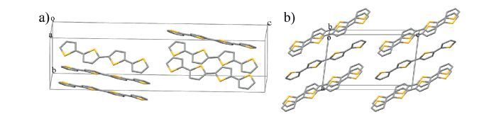
Polymorphism also represents a crucial issue for tetrathiafulvalenes (TTFs). We obtained controllably the parent compound TTF crystalsofα-andβ-phasesbydropcastingmethodwiththe selection of different solvents [10]. Thehighestfield-effectmobility ofα-phase single crystals reached 1.2 cm2 V-1 s-1, while β-phase single crystals showedthemaximummobility assmall as0.23 cm2 V-1 s-1. -1. The superior charge transport behaviour of α-phase single crystals could be attributed to the strong π-π interactions along the short b axis and the short contacts between S atoms.
Brillante et al. found that dibenzotetrathiafulvalene (DB-TTF) presented four polymorphic modifications at ambient conditions [51]. Pure α-phase crystals were achieved at room temperature by crystallization from hot chlorobenzene and DMF solutions, as well as by drop casting on Si/SiO2 from hot chlorobenzene. Single crystals of β-phase were prepared by recrystallization from a saturated solution in hot toluene, always mixed with α-phase crystals. The g-phase was identified in DB-TTF films deposited by either UHV vapour deposition on SiO2 substrates or drop casting of colloidal composite of polystyrene beads and DB-TTF. A fourth polymorph, the pure δ-phase, was obtained by crystallization from a mixture of isopropanol and nitromethane as well as by vacuum vapour deposition. Only singly crystal structures of α-phase and bphase were well resolved to provide detailed information about packing structure (Fig. 7). For α-phase, almost planar molecules of DB-TTF stack along the b axis with an interplanar distance of 3.545 Å forming a herringbone structure with an angle of 52.648. The crystal structure in the case of β-phase shows also a herringbone motif in which the molecules have edge-to-face packing with an angle of 52.228 between the mean planes of the molecules. However, there is neither π-π overlap between consecutive molecules in the stacks along b nor short contacts between adjacent columns, in contrast with the α-phase. Thus, solution-prepared single crystal OFETs based on α-phase as active materials showed best hole mobility of up to 1.0 cm2 V-1 s-1 [52].
Solution-prepared single crystal field-effect transistors based on α-phase of dithiophene-tetrathiafulvalene (DT-TTF) showed a hole mobility of up to 3.6 cm2 V-1 s-1 [53, 54]. Mas-Torrent found a new polymorph, namely β-phase, which showed a much lower mobility up to 0.17 cm2 V-1 s-1 compared with α-phase (Fig. 8) [11]. Long plate crystals of α-phase can be easily prepared from a variety of solutions [53-55] The hexagonal-shaped platelets of bphase were grown on some substrates from a solution of toluene or dichlorobenzene, mixed with crystals of the α-phase. However, by ultrasonication of the solution before drop casting, the relative ratio of b-DT-TTF increased, whereas the α-phase was mostly obtained in presence of small seed crystals. This indicates that the crystallization of α-phase probably starts in the solution while the β-phase crystallizes directly on the substrate. The crystallographic studies revealed that both phases show a similar crystal structure, but distances between neighbouring molecules are larger for bphase single crystals, which is responsible for the big difference in device performance.
2.7. OligothiophenesThe α-oligothiophene compounds nT (n = 2-8) is an important class of organic semiconductors for electronic devices [56-58]. All non-substituted α-nTs crystal structures belong to the monoclinic system with a P21 space group. Although α-5T and α-8T only showed a unique crystallographic phase till now, two different crystal polymorphs have been observed for α-3T [59], α-4T [12, 13] and α-6T [14, 60, 61]. In the two cases of α-4T (Fig. 9) and α-6T, high-temperature (HT) phase forms packs with Z = 2 while lowtemperature (LT) phase adopts a Z = 4 structure. Both phases of α- 4T and α-6T can be grown by vapour transport [12, 61] whereas LT phase of α-4T can be achieved by solution techniques [62] due to much higher solubility of α-4T relative to α-6T. For example, a novel floating-drop technique was employed for the growth of centimetre-sized LT phase single crystals of α-4T by the isothermal evaporation of the solvent using water as liquid substrate [62]. Solid-solid phase transitions from LT to HT polymorph for both α- 4T and α-6T were also demonstrated to occur in heating conditions [63-65]. α-4T thin films grown by organic molecular beam epitaxy (OMBE) showed a metastable structure in the first stage even when deposition was carried out at room temperature and then evolved to the LT phase in the post deposition stage [66]. The HT phase of α- 4T, due to its higher carrier mobility with larger dispersion of the HOMOs, is considered as the most promising polymorph of 4T for applications in organic devices [12, 67]. Epitaxial α-4T films can be grown on single crystal pentaerythritol, where a pseudomorphic phase close to HT phase grows as the dominant film phase [68]. This is the first time that a quasi-HT polymorph was observed in thin films grown at room temperature.

|
Download:
|
| Figure 7. Crystal structure of the α-phase (a) and β-phase (b) of DB-TTF. | |

|
Download:
|
| Figure 8. Optical microscope images of single crystal field-effect transistor based on b- DT-TTF and α-DT-TTF. Inset shows the molecular structure of DT-TTF. Reprinted with permission from Ref. [11], Copyright 2014, Wiley-VCH. | |

|
Download:
|
| Figure 9. Crystal structure of the LT phase (a) and HT phase (b) of α-4T. | |
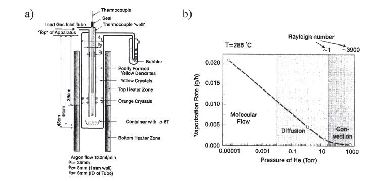
α-6T based field-effect transistors show a much high carrier mobility compared with α-4T probably owing to longer conjugation length. Its mobility is improved from 10-4 cm2 V-1 s-1 to 0.16 cm2 V-1 s-1 within the past few decades [58, 69, 70]. Laudise et al. succeeded in growing 500 mm HT phase of α-6T single crystals from the melt contained in a small capillary by a slow cool speed (0.1 ℃ min-1) or quenched procedure using 30 mg of the material [63]. Later centimetre-sized crystals of α-6T were obtained by physical vapour transport in the convective regime (Fig. 10) [71]. HT or LT modification deposited and grew at temperature above or below 250 ℃, respectively, and 1 atm inert gas was utilized to repress nucleation and set the system in the convective regime. Cellular circulation was important to provide isothermal depositions over large regions, thus leading to a separation of LT and HT growth regions. Bao et al. demonstrated that an SiO2 surface with patterned Au films can act as an effective template which not only allows the vapour deposition of LT phase of α-6T on designed locations but also flat geometry and welldefined sizes and shapes. Top-contact FETs fabricated with ribbonlike α-6T crystals exhibited a mobility as high as 0.1 cm2 V-1 s-1.

|
Download:
|
| Figure 10. (a) Furnace and glass apparatus for α-6T transport and crystal growth; (b) Evaporation rate of α-6T as a function of inert-gas pressure. Reprinted with permission from Ref. [71], Copyright 1997, Elsevier Science B.V. | |
2.8. Naphthalene diimide
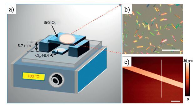
Naphthalene diimide (NDI)-based field-effect transistors have demonstrated outstanding n-type semiconductivity because of a large electron affinity and close π-stacking [72-77].Wu¨ rthner et al.demonstrated that single-crystal transistors based on α-phase of N, N’-bis-(heptafluorobutyl)-2, 6-dichloro-1, 4, 5, 8-naphthalene tetracarboxylic diimide (Cl2-NDI) showed the mobility up to 8.6 cm2 V-1 s-1, which is the best performance for air stable ntype single crystal transistors reported till now [76]. The α-phase ribbon-shaped Cl2-NDI crystals were grown on n-octadecyl triethoxysilane modified substrate by drop-casting of CHCl3 solution. Later β-phase ribbon-shaped crystals with tens of micrometre size were grown on various substrates like Si/SiO2 by sublimation at ambient pressure in air (Fig. 11) [77]. The versatility of such simple sublimation in air was further demonstrated by the deposition of highly crystalline thin films with large domain sizes on a SiO2 wafer. The single crystal and thin film transistors based on b-Cl2-NDI showed mobilities of 3.5 and 0.37 cm2 V-1 s-1, respectively.

|
Download:
|
| Figure 11. Single crystal growth by simple sublimation in air. (a) Schematic drawing of the applied setup for crystal growth on Si/SiO2 substrates. (b) Optical microscopy image of the β-phase single crystals grown on Si/SiO2 substrate. Scale bar, 200 mm. (c) AFM image and cross-section thickness analysis of a representative single crystal. Scale bar, 2 mm. Reprinted with permission from Ref. [78], Copyright 2015, Macmillan Publishers Limited. | |
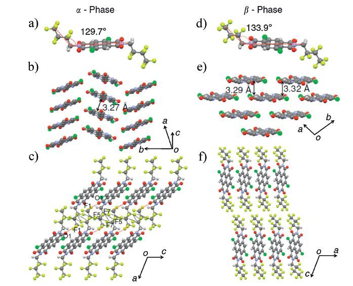
The solid-to-solid transition from α-phase to β-phase occurred at a temperature around 180 ℃, indicating that β-phase crystals are the thermodynamically favoured polymorph at elevated temperature. The colourless α-phase crystals belong to the monoclinic space group P21/c with Z = 2 while yellow β-phase crystals belong to the triclinic space group P-1 with Z = 1 (Fig. 12). The α-phase crystals take a herringbone packing motif where nearly half of each NDI molecular skeleton overlaps with the adjacent molecule at a close π-stack distance of 3.27 Å . On the other hand, β-phase molecules exhibit a two-dimensional brickwall packing arrangement with a π-stack distance of 3.29 and 3.32 Å . In contrast to the more tilted arrangement on the substrate for α-phase, β-phase molecules are standing upright along the current direction. By its two-dimensional brick-wall packing and the resulting slipping angles, the β-phase exhibits a weaker electronic coupling between the π-scaffolds of neighbouring molecules and a longer percolation pathway for electrons to cross the unit cell compared with the α-phase with its more directional coupling and transport along the π-stacks. Therefore, the α-phase showed much high hole mobility than β-phase.

|
Download:
|
| Figure 12. Crystal structures of both polymorphs at 100 K. Molecular structure of Cl2-NDI in (a) α-phase and (d) β-phase. Crystal packing structures of (b) herringbone packing mode with π-π distance of 3.27 Å and the slipping angle of 6$\overset{\circ }{\mathop{2}}\,$ for α-phase, and (e) two-dimensional brick-wall packing with π-π distances of 3.29 and 3.32 Å in the (ab)- plane, corresponding to slipping angles of 4 $\overset{\circ }{\mathop{1}}\,$ and 3 $\overset{\circ }{\mathop{2}}\,$ for β-phase, respectively (for clarity, -CH2C3F7 omitted). Crystal packing structures of (c) α-phase and (f) β-phase Cl2-NDI with tilt angles of about 6$\overset{\circ }{\mathop{7}}\,$ and 9$\overset{\circ }{\mathop{0}}\,$ on the substrate, respectively. The red, green, blue, grey, white and yellow coloured atoms represent O, Cl, N, C, H and F, respectively. Reprinted with permission from Ref. [77], copyright 2015, Macmillan Publishers Limited. | |
3. Conclusion and outlook
In this short review, we have emphasized the significant role of polymorph control of organic materials in the carrier mobility of field-effect transistors. First of all, special techniques such as solution sheared method, organic molecular beam epitaxy or micro melt technique can be utilized to achieve superior mobility phase for a lot of promising organic semiconductors, whose crystal polymorph has not been investigated yet. Especially for n-type semiconductors, the investigation of the relationship between crystal phase and electronic performance can provide insights into the construction of high-performance devices, which is highly demanding to develop ambipolar transistors and complementary circuits [78]. Second, it still remains a big challenge to precisely tailor thermodynamic and kinetic factors of crystal nucleation and growth towards defined crystal phase for large area thin film with good morphology or high quality single crystals with uniform size in fabrication of high-performance thin film or single crystal transistors. Third, there is a long way to go before revealing a clear relationship between molecular structure and crystal polymorph where the functional units influence remarkably the pathways of molecular recognition and the behaviours of self assembly. It is essential for rational design of molecular structures of organic semiconductors to present desired crystal polymorph with outstanding electrical characteristics.
Acknowledgments The authors acknowledge financial support from the Ministry of Science and Technology of China (Nos. 2013CB933504, 2014CB643600, 2015CB856502), the National Natural Science Foundation of China (Nos. 91222203, 51303185, 21473222), the Strategic Priority Research Program (No. XDB12000000) and the Youth Innovation Promotion Association (Chinese Academy of Sciences)| [1] | W.C. McCrone, Polymorphism, in: D. Fox, M.M. Labes, A. Weissberger (Eds.), Physics and Chemistry of the Organic Solid State, 2, Interscience, New York, 1965, pp. 725-767. |
| [2] | G.R. Desiraju. Polymorphism: the same and not quite the same. Cryst. Growth Des. 8 (2008) 3–5. DOI:10.1021/cg701000q |
| [3] | T.L. Threlfall. Analysis of organic polymorphs. A review. Analyst 120 (1995) 2435–2460. DOI:10.1039/an9952002435 |
| [4] | J.D. Dunitz. Phase transitions in molecular crystals from a chemical viewpoint. Pure Appl. Chem. 63 (1991) 177–185. |
| [5] | Liebig Wöhler. Untersuchungen über das Radikal der Benzoesäure. Ann. Pharm. 3 (1832) 249–282. DOI:10.1002/(ISSN)1099-0690 |
| [6] | L.W. Huang, Q. Liao, Q. Shi, et al. Rubrene micro-crystals from solution routes: their crystallography, morphology and optical properties. J. Mater. Chem. 20 (2010) 159–166. DOI:10.1039/B914334C |
| [7] | R. Ruiz, D. Choudhary, B. Nickel, et al. Pentacene thin film growth. Chem. Mater. 16 (2004) 4497–4508. DOI:10.1021/cm049563q |
| [8] | C.C. Mattheus, G.A. de Wijs, R.A. de Groot, T.T.M. Palstra. Modeling the polymorphism of pentacene. J. Am. Chem. Soc. 125 (2003) 6323–6330. DOI:10.1021/ja0211499 |
| [9] | L. Li, Q. Tang, H. Li, et al. An ultra closely π-stacked organic semiconductor for high performance field-effect transistors. Adv. Mater. 19 (2007) 2613–2617. DOI:10.1002/(ISSN)1521-4095 |
| [10] | H. Jiang, X.J. Yang, Z.D. Cui, et al. Phase dependence of single crystalline transistors of tetrathiafulvalene. Appl. Phys. Lett. 91 (2007) 123505. DOI:10.1063/1.2784970 |
| [11] | R. Pfattner, M. Mas-Torrent, I. Bilotti, et al. High-performance single crystal organic field-effect transistors based on two dithiophene-tetrathiafulvalene (DT-TTF) polymorphs. Adv. Mater. 22 (2010) 4198–4203. DOI:10.1002/adma.v22:37 |
| [12] | T. Siegrist, C. Kloc, R.A. Laudise, H.E. Katz, R.C. Haddon. Crystal growth, structure, and electronic band structure of alpha-4 T polymorphs. Adv. Mater. 10 (1998) 379–382. DOI:10.1002/(ISSN)1521-4095 |
| [13] | L. Antolini, G. Horowitz, F.F. Kouki, F. Garnier. Polymorphism in oligothiophenes with an even number of thiophene subunits. Adv. Mater. 10 (1998) 382–385. DOI:10.1002/(ISSN)1521-4095 |
| [14] | B. Servet, G. Horowitz, S. Ries, et al. Polymorphism and charge transport in vacuum-evaporated sexithiophene films. Chem. Mater. 6 (1994) 1809–1815. DOI:10.1021/cm00046a039 |
| [15] | C.D. Dimitrakopoulos, P.R.L. Malenfant. Organic thin film transistors for large area electronics. Adv. Mater. 14 (2002) 99–117. DOI:10.1002/(ISSN)1521-4095 |
| [16] | N. Karl. Charge carrier transport in organic semiconductors. Synth. Met. 133-134 (2003) 649–657. DOI:10.1016/S0379-6779(02)00398-3 |
| [17] | G.R. Desiraju. Cryptic crystallography. Nat. Mater. 1 (2002) 77–79. DOI:10.1038/nmat726 |
| [18] | A.L. Briseno, S.C.B. Mannsfeld, M.M. Ling, et al. Patterning organic single-crystal transistor arrays. Nature 444 (2006) 913–917. DOI:10.1038/nature05427 |
| [19] | J. Bernstein, R.J. Davey, J.O. Henck. Concomitant polymorphs. Angew. Chem. Int. Ed. 38 (1999) 3440–3461. DOI:10.1002/(SICI)1521-3773(19991203)38:23<>1.0.CO;2-U |
| [20] | V.C. Sundar, J. Zaumseil, V. Podzorov, et al. Elastomeric transistor stamps: reversible probing of charge transport in organic crystals. Science 303 (2004) 1644–1646. DOI:10.1126/science.1094196 |
| [21] | V. Podzorov, E. Menard, A. Borissov, et al. Intrinsic charge transport on the surface of organic semiconductors. Phys. Rev. Lett. 93 (2004) 086602. DOI:10.1103/PhysRevLett.93.086602 |
| [22] | D.E. Henn, W.G. Williams, D.J. Gibbons. Crystallographic data for an orthorhombic form of rubrene. J. Appl. Crystallogr. 4 (1971) 256. DOI:10.1107/S0021889871006812 |
| [23] | O.D. Jurchescu, A. Meetsma, T.T.M. Palstra. Low-temperature structure of rubrene single crystals grown by vapor transport. Acta Crystallogr. B 62 (2006) 330–334. DOI:10.1107/S0108768106003053 |
| [24] | J. Takeya, M. Yamagishi, Y. Tominari, et al. Very high-mobility organic singlecrystal transistors with in-crystal conduction channels. Appl. Phys. Lett. 90 (2007) 102120. DOI:10.1063/1.2711393 |
| [25] | J.L. Brédas, J.P. Calbert, D.A. da Silva, J. Cornil. Organic semiconductors: a theoretical characterization of the basic parameters governing charge transport. Proc. Natl. Acad. Sci. USA 99 (2002) 5804–5809. DOI:10.1073/pnas.092143399 |
| [26] | D.A. da Silva, E.G. Kim, J.L. Brédas. Transport properties in the rubrene crystal: electronic coupling and vibrational reorganization energy. Adv. Mater. 17 (2005) 1072–1076. DOI:10.1002/adma.v17:8 |
| [27] | T. Matsukawa, M. Yoshimura, K. Sasai, et al. Growth of thin rubrene single crystals from 1-propanol solvent. J. Cryst. Growth 312 (2010) 310–313. DOI:10.1016/j.jcrysgro.2009.10.048 |
| [28] | C.H. Lee, T. Schiros, E.J.G. Santos, et al. Epitaxial growth of molecular crystals on van der Waals substrates for high-performance organic electronics. Adv. Mater. 26 (2014) 2812–2817. DOI:10.1002/adma.v26.18 |
| [29] | S.E. Fritz, S.M. Martin, C.D. Frisbie, et al. Structural characterization of a pentacene monolayer on an amorphous SiO2 substrate with grazing incidence X-ray diffraction. J. Am. Chem. Soc. 126 (2004) 4084–4085. DOI:10.1021/ja049726b |
| [30] | L.F. Drummy, D.C. Martin. Thickness-driven orthorhombic to triclinic phase transformation in pentacene thin films. Adv. Mater. 17 (2005) 903–907. DOI:10.1002/(ISSN)1521-4095 |
| [31] | H.L. Cheng, Y.S. Mai, W.Y. Chou, L.R. Chang, X.W. Liang. Thickness-dependent structural evolutions and growth models in relation to carrier transport properties in polycrystalline pentacene thin films. Adv. Funct. Mater. 17 (2007) 3639–3649. DOI:10.1002/(ISSN)1616-3028 |
| [32] | A. Brillante, I. Bilotti, R.G.D. Valle, et al. Characterization of phase purity in organic semiconductors by lattice-phonon confocal Raman mapping: application to pentacene. Adv. Mater. 17 (2005) 2549–2553. DOI:10.1002/(ISSN)1521-4095 |
| [33] | S. Schiefer, M. Huth, A. Dobrinevski, B. Nickel. Determination of the crystal structure of substrate-induced pentacene polymorphs in fiber structured thin films. J. Am. Chem. Soc. 129 (2007) 10316–10317. DOI:10.1021/ja0730516 |
| [34] | M.H. Chang, W.Y. Chou, Y.C. Lee, et al. Polymorphic transformation induced by nanoimprinted technology in pentacene-film early-stage growth. Appl. Phys. Lett. 97 (2010) 183301. DOI:10.1063/1.3512863 |
| [35] | C.H. Wang, C.Y. Hsieh, J.C. Hwang. Flexible organic thin-film transistors with silk fibroin as the gate dielectric. Adv. Mater. 23 (2011) 1630–1634. DOI:10.1002/adma.201004071 |
| [36] | I.P.M. Bouchoms, W.A. Schoonveld, J. Vrijmoeth, T.M. Klapwijk. Morphology identification of the thin film phases of vacuum evaporated pentacene on SiO2 substrates. Synth. Met. 104 (1999) 175–178. DOI:10.1016/S0379-6779(99)00050-8 |
| [37] | J.E. Anthony, J.S. Brooks, D.L. Eaton, S.R. Parkin. Functionalized pentacene: improved electronic properties from control of solid-state order. J. Am. Chem. Soc. 123 (2001) 9482–9483. DOI:10.1021/ja0162459 |
| [38] | S.C. B.Mannsfeld, M.L. Tang, Z.N. Bao. Thin film structure of triisopropylsilylethynyl-functionalized pentacene and tetraceno[2, 3-b]thiophene from grazing incidence X-ray diffraction. Adv. Mater. 23 (2011) 127–131. DOI:10.1002/adma.v23.1 |
| [39] | G. Giri, E. Verploegen, S.C.B. Mannsfeld, et al. Tuning charge transport in solutionsheared organic semiconductors using lattice strain. Nature 480 (2011) 504–508. DOI:10.1038/nature10683 |
| [40] | K. Takimiya, I. Osaka, T. Mori, M. Nakano. Organic semiconductors based on[1] benzothieno[3, 2-b][1] benzothiophene substructure. Acc. Chem. Res. 47 (2014) 1493–1502. DOI:10.1021/ar400282g |
| [41] | K. Takimiya, S. Shinamura, I. Osaka, E. Miyazaki. Thienoacene-based organic semiconductors. Adv. Mater. 23 (2011) 4347–4370. DOI:10.1002/adma.201102007 |
| [42] | Z.N. Bao, A.J. Lovinger, A. Dodabalapur. Organic field-effect transistors with high mobility based on copper phthalocyanine. Appl. Phys. Lett. 69 (1996) 3066–3068. DOI:10.1063/1.116841 |
| [43] | R. Zeis, T. Siegrist, C. Kloc. Single-crystal field-effect transistors based on copper phthalocyanine. Appl. Phys. Lett. 86 (2005) 022103. DOI:10.1063/1.1849438 |
| [44] | N.M. Bamsey, A.P. Yuen, A.M. Hor, et al. Integration of an M-phthalocyanine layer into solution-processed organic photovoltaic cells for improved spectral coverage. Sol. Energ. Mat. Sol. C 95 (2011) 1970–1973. DOI:10.1016/j.solmat.2011.01.042 |
| [45] | D. Placencia, W.N. Wang, R.C. Shallcross, et al. Organic photovoltaic cells based on solvent-annealed, textured titanyl phthalocyanine/C60 heterojunctions. Adv. Funct. Mater. 19 (2009) 1913–1921. DOI:10.1002/adfm.v19:12 |
| [46] | T. Del Caño, V. Parra, M.L. Rodríguez-Méndez, et al. Characterization of evaporated trivalent and tetravalent phthalocyanines thin films: different degree of organization. Appl. Surf. Sci. 246 (2005) 327–333. DOI:10.1016/j.apsusc.2004.11.036 |
| [47] | M. Brinkmann, J.C. Wittmann, M. Barthel, M. Hanack, C. Chaumont. Highly ordered titanyl phthalocyanine films grown by directional crystallization on oriented poly(tetrafluoroethylene) substrate. Chem. Mater. 14 (2002) 904–914. DOI:10.1021/cm011241o |
| [48] | H. Yonehara, H. Etori, M.K. Engel, et al. Fabrication of various ordered films of oxotitanium(IV) phthalocyanine by vacuum deposition and their spectroscopic behavior. Chem. Mater. 13 (2001) 1015–1022. DOI:10.1021/cm000766y |
| [49] | W.C. Chen, L.Z. Huang, X.L. Qiao, et al. Efficient planar organic solar cells with the high near-infrared response. Org. Electron. 13 (2012) 1086–1091. DOI:10.1016/j.orgel.2012.03.002 |
| [50] | Z.P. Zhang, L. Jiang, C.L. Cheng, et al. The impact of interlayer electronic coupling on charge transport in organic semiconductors: a case study on titanylphthalocyanine single crystals. Angew. Chem. Int. Ed. 55 (2016) 5206–5209. DOI:10.1002/anie.201601065 |
| [51] | A. Brillante, I. Bilotti, R.G.D. Valle, et al. The four polymorphic modifications of the semiconductor dibenzo-tetrathiafulvalene. Crystengcomm 10 (2008) 1899–1909. DOI:10.1039/b810993a |
| [52] | M. Mas-Torrent, P. Hadley, S.T. Bromley, N. Crivillers. Single-crystal organic fieldeffect transistors based on dibenzo-tetrathiafulvalene. Appl. Phys. Lett. 86 (2005) 012110. DOI:10.1063/1.1848179 |
| [53] | M. Mas-Torrent, M. Durkut, P. Hadley, X. Ribas, C. Rovira. High mobility of dithiophene-tetrathiafulvalene single-crystal organic field effect transistors. J. Am. Chem. Soc. 126 (2004) 984–985. DOI:10.1021/ja0393933 |
| [54] | M. Leufgen, O. Rost, C. Gould, et al. High-mobility tetrathiafulvalene organic fieldeffect transistors from solution processing. Org. Electron. 9 (2008) 1101–1106. DOI:10.1016/j.orgel.2008.08.011 |
| [55] | M. Mas-Torrent, P. Hadley, X. Ribas, C. Rovira. Temperature dependence of the electrical properties of single-crystals of dithiophene-tetrathiafulvalene (DTTTF). Synth. Met. 146 (2004) 265–268. DOI:10.1016/j.synthmet.2004.08.023 |
| [56] | D. Fichou. Structural order in conjugated oligothiophenes and its implications on opto-electronic devices. J. Mater. Chem. 10 (2000) 571–588. DOI:10.1039/a908312j |
| [57] | L. Zhang, N.S. Colella, B.P. Cherniawski, et al. Oligothiophene semiconductors: synthesis, characterization, and applications for organic devices, ACS Appl. Mater. Interfaces. 6 (2014) 5327–5343. DOI:10.1021/am4060468 |
| [58] | M. Halik, H. Klauk, U. Zschieschang, et al. Relationship between molecular structure and electrical performance of oligothiophene organic thin film transistors. Adv. Mater. 15 (2003) 917–922. DOI:10.1002/adma.200304654 |
| [59] | G. Schweicher, N. Paquay, C. Amato, et al. Toward single crystal thin films of terthiophene by directional crystallization using a thermal gradient. Cryst. Growth Des. 11 (2011) 3663–3672. DOI:10.1021/cg2007793 |
| [60] | T. Siegrist, R.M. Fleming, R.C. Haddon, et al. The crystal structure of the hightemperature polymorph of a-hexathienyl (a-6 T/HT). J. Mater. Res. 10 (1995) 2170–2173. DOI:10.1557/JMR.1995.2170 |
| [61] | G. Horowitz, B. Bachet, A. Yassar, et al. Growth and characterization of sexithiophene single crystals. Chem. Mater. 7 (1995) 1337–1341. DOI:10.1021/cm00055a010 |
| [62] | M. Campione, R. Ruggerone, S. Tavazzi, M. Moret. Growth and characterisation of centimetre-sized single crystals of molecular organic materials. J. Mater. Chem. 15 (2005) 2437–2443. DOI:10.1039/b415912h |
| [63] | R.A. Laudise, P.M. Bridenbaugh, T. Siegrist, et al. Growth of α-hexathienyl by a micro melt technique. J. Cryst. Growth 152 (1995) 241–244. DOI:10.1016/0022-0248(95)00134-4 |
| [64] | S. Destri, M. Mascherpa, W. Porzio. Mesophase formation in α-sexithienyl at high temperature-an X-ray diffraction study. Adv. Mater. 5 (1993) 43–45. DOI:10.1002/(ISSN)1521-4095 |
| [65] | M. Campione, S. Tavazzi, M. Moret, W. Porzio. Crystal-to-crystal phase transition in a-quaterthiophene: an optical and structural study. J. Appl. Phys. 101 (2007) 083512. DOI:10.1063/1.2718291 |
| [66] | M. Campione, A. Borghesi, M. Laicini, et al. Growth-related properties and postgrowth phenomena in organic molecular thin films. J. Chem. Phys. 127 (2007) 244703. DOI:10.1063/1.2814244 |
| [67] | A. Sassella, D. Braga, M. Campione, et al. Probing phase transitions and stability of organic semiconductor single crystals by dielectric investigation. J. Appl. Phys. 109 (2011) 013529. DOI:10.1063/1.3531574 |
| [68] | S.E. Kaviyil, M. Campione, A. Sassella, et al. Growth of pseudomorphic structures through organic epitaxy. J. Chem. Phys. 137 (2012) 224703. DOI:10.1063/1.4770001 |
| [69] | C.L. Wang, H.L. Dong, W.P. Hu, Y.Q. Liu, D.B. Zhu. Semiconducting π-conjugated systems in field-effect transistors: a material odyssey of organic electronics. Chem. Rev. 112 (2012) 2208–2267. DOI:10.1021/cr100380z |
| [70] | G. Horowitz, R. Hajlaoui, F. Kouki. An analytical model for the organic field-effect transistor in the depletion mode. Application to sexithiophene films and single crystals. Eur. Phys. J. Appl. Phys. 1 (1998) 361–367. DOI:10.1051/epjap:1998157 |
| [71] | C. Kloc, P.G. Simpkins, T. Siegrist, P.A. Laudise. Physical vapor growth of centimeter-sized crystals of a-hexathiophene. J. Cryst. Growth 182 (1997) 416–427. DOI:10.1016/S0022-0248(97)00370-9 |
| [72] | H.E. Katz, A.J. Lovinger, J. Johnson, et al. A soluble and air-stable organic semiconductor with high electron mobility. Nature 404 (2000) 478–481. DOI:10.1038/35006603 |
| [73] | J.H. Oh, S.L. Suraru, W.Y. Lee, et al. High-performance air-stable n-type organic transistors based on core-chlorinated naphthalene tetracarboxylic diimides. Adv. Funct. Mater. 20 (2010) 2148–2156. DOI:10.1002/adfm.v20:13 |
| [74] | H. Usta, A. Facchetti, T.J. Marks. n-channel semiconductor materials design for organic complementary circuits. Acc. Chem. Res. 44 (2011) 501–510. DOI:10.1021/ar200006r |
| [75] | F.J. Zhang, Y.B. Hu, T. Schuettfort, et al. Critical role of alkyl chain branching of organic semiconductors in enabling solution-processed N-channel organic thinfilm transistors with mobility of up to 3.50 cm2 V-1 s-1. J. Am. Chem. Soc. 135 (2013) 2338–2349. DOI:10.1021/ja311469y |
| [76] | T. He, M. Stolte, F. Würthner. Air-stable n-channel organic single crystal fieldeffect transistors based on microribbons of core-chlorinated naphthalene diimide. Adv. Mater. 25 (2013) 6951–6955. DOI:10.1002/adma.v25.48 |
| [77] | T. He, M. Stolte, C. Burschka, et al. Single-crystal field-effect transistors of new Cl2-NDI polymorph processed by sublimation in air. Nat. Commun. 6 (2015) 5954. DOI:10.1038/ncomms6954 |
| [78] | J. Zaumseil, H. Sirringhaus. Electron and ambipolar transport in organic fieldeffect transistors. Chem. Rev. 107 (2007) 1296–1323. DOI:10.1021/cr0501543 |