 2016, Vol. 27


Molecular electronics seeks to utilize single molecules and their assemblies as active components to achieve electronic functions (e.g.,switching,rectifying) [1, 2].he central task in this field is to explore the charge transport behaviors and molecular functionalities at the single-molecule level. Since the pioneering studies in the 1970s [3, 4],a variety of organic molecules have been specifically designed and tested as potential candidate materials [1, 2, 5],which greatly contributed to our understanding on the molecular structure-transport-function relationships.
Conjugated polymers (CPs) have demonstrated their successful applications in organic electronics,benefitting from their outstanding optoelectronic properties,easy processability and good chemical stability [6]. Recently they are also considered a class of potential candidates formolecular electronics.More significantly,CPs possess some unique features compared to small molecules.Firstly,the long conjugated chain may enable CPs to mediate long-range charge transport.his capability is the key for a molecule to function as a molecular wire in electronic circuits. Secondly,the long polymeric structure offers enough room for various functional units/substituents to be integrated into single molecules,thus tailor-made CPs can also be utilized as active components in molecular devices.
So far,however,the core materials for molecular electronics have been mostly limited to small molecules (molecular length within several nanometers) [7, 8],while very few studies have incorporated CPs into molecular junctions. On one hand,their extra-long structures and the rather complex,strong interchain interactions make it technologically challenging to fix isolated polymeric chains into junctions or to assemble them into a well organized monolayer on electrode surface,resulting in generally low device yields. On the other hand,the understanding of charge transport over long pathways is still limited and more work is needed to clarify the electronic properties of CPs at the molecular scale.or example,it has been observed that current normally decays evidently with molecular length [9, 10],and CPs are proposed to be ideal candidates that can effectively mediate charge transport over distance ranging from tens to hundreds of nanometers,but how to optimize molecular electronic structures of CPs for this aim remains an open question.
Although CP-based molecular electronics is less studied,remarkable progress has been achieved in the last decade or so. Here we are motivated to present this review,showing how the above-mentioned challenges have been addressed and summarizing the transport behaviors of CPs as well as their electronic functions.his review will focus on three issues: (1) the methods to construct molecular junctions with CPs as core components,(2) the charge transport behaviors of CPs and (3) the potential applications of CPs in molecular-scale electronic devices.risbie et al. provided an excellent review on transport through long conjugated molecules five years ago [7],here we focus on polymers that are even longer (normally above 15 nm),highlighting the recent progress in this field. Polymeric ultrathin-film organic fieldeffect transistors are beyond the scope of this review.
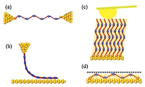
2. Construction of molecular-scale CP junctionsThe first step toward molecular electronics study is to sandwich single molecules or monolayered molecules between electrodes,forming metal/molecule/metal junctions.ue to their ultra-long length,arranging CPs into molecular junction is a rather challenging task. Nevertheless,several reliable methods have been developed for constructing CP junctions.hese methods include bridging CP chains between nanogap electrodes,pulling isolated polymers with STM tip and assembly of CPs into a monolayer on bottom electrodes with subsequent top contacts. As for monolayered CP junctions,CPs either stand vertically or lie flat on a substrate.he representative structures are shown in Fig. 1.

|
Download:
|
| Figure 1. Representative architectures of CP junctions. (a) Nanogap electrodes bridged by CP chain(s). (b) A single CP chain pulled by STM tip. (c) Vertical monolayer junction with the probe of CAFM as top contact. (d) Planar monolayer junction with graphene as top contact. | |
2.1. Nanogap electrodes
Nanogap electrodes,namely a pair of electrodes with a nanometer gap,represent a fundamental platform for fabricating metal/molecule/metal devices [11]. With nanogap electrodes,molecular-scale CP junctions have been successfully constructed.
The first attempt to construct single-chain junction was made by Tao and co-workers [12],who were able to connect Au nanogaps by in situ polymerization (Fig. 2a). Aniline or pyrrole monomers were polymerized in electrolyte through potential cycling and the process could be monitored by current. Once polymers bridged the gap,the current between the nanoelectrodes jumped up 2-3 orders of magnitude and the potential cycling was stopped immediately to minimize the amount of polymer chains. In this way,the polymers bridging the nanogap were limited to only a few chains and even a single chain. Random on-off telegraphic switching was observed,attributed to the act of a single polymer strand.

|
Download:
|
| Figure 2. Schematics of bridging CP wires between nanogap electrodes. (a) In situ growth of polyaniline or polypyrrole between the nanogap [12]. (b) A three-step interconnection method to wire CPs into gap electrodes [13]. (c) Self-assembly of porphyrin polymers into nanogap junctions [14]. (d) Self-assembly of single-chain PPE between the nanoelectrodes [15]. (a) Adapted with permission from [12]. Copyright 2003 American Physical Society. (b) Adapted with permission from [13]. Copyright 2006 American Chemical Society. (c) Adapted with permission from [14]. Copyright 2009 Royal Society of Chemistry. (d) Adapted with permission from [15]. Copyright 2006 American Physical Society. | |
Taniguchi et al. [13] developed a stepwise interconnection method to bridge CPs between nanogap electrodes (Fig.b).he method was a simple solution process,including three sequential reactions between building blocks: (1) self-assembly of “initiator” molecules on two electrode surfaces,(2) grafting of π-oligomers onto the initiators,and (3) interconnecting both ends of the oligomers with a linker core to form a junction.he 30 nm gap was estimated to be bridged by an ensemble of ~450 molecules in parallel.he electrical properties of the junction could be designed by using appropriate component molecules.or example,using diarylethene,a photo-responsive molecule,as linker core produced a photoswitchable molecular junction.
It is also possible to directly assemble as-prepared CPs into electrode gaps if the CPs are equipped with anchoring groups.n Ozawa’ s work [14],17-nm-long porphyrin polymers bearing thiol end-capping groups were assembled into a 10-nm gap (Fig.c). Successful bridging led to clearly increased conductivity of the junction.ullerenes were further decorated onto poly (porphyrin)s in the junction via pyridine-Zn coordination,by soaking the junction into a solution of fullerenes modified with pyridine moieties.he direct assembly of end-modified polymers into nanogap is a straightforward and convenient method.t is noteworthy that,during the self-assembly process,the molecules have adsorption interactions with both electrode surfaces and are forced to adopt a certain tilt angle to bridge the gap,therefore the molecular arrangement and conformation in the gap need to be clarified for a better understanding of the device performance.
Hu et al. assembled thiol-end-capped poly(π-πhenyleneethynylene) (PPE) into nanogap electrodes and simultaneously monitored the current across the gap (Fig.d) [15]. As soon as one polymer molecule was trapped,the current jumped to a new value.t has been observed that 19 jumps appeared during 130 h self-assembly process and a connected nanowire with diameter of -20 nm was finally obtained.o limit the number of CPs in the junction,self-assembly process was stopped as soon as the first current jump was observed.n this way CPs assembled into junction could be limited down to even a single chain.n addition,the gap electrodes prepared by electroplating method could match the length of the rigid PPE backbones,which favored the formation of single-chain junction.
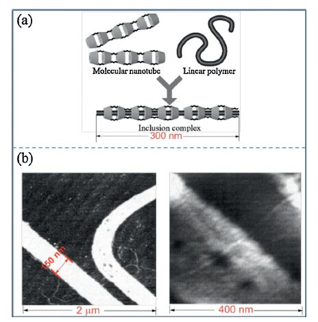
Encapsulating CPs with an insulating sheath yields so-called insulated molecular wires (IMWs) [16-18].he presence of the insulating layer can effectively reduce the interchain interactions,and also enhance the rigidity of CP backbone by restricting the intramolecular motions [19-22],which are in favor of building single-chain junctions. As an example,MWs were prepared by inclusion of as-prepared polyaniline within cyclodextrin molecular nanotube (Fig. 3a) [19],and the conductivity of a singleMW was measured by using narrow-gap (150 nm) Pt electrodes fabricated by scanning-probe nanofabrication (Fig. 3b) [23]. Although the insulating layer brings extra tunneling barrier at the polymer/ electrode contact,the extra contact resistance is not large compared to the intrinsic resistance of the polymer [23].

|
Download:
|
| Figure 3. (a) Preparation of an IMW composed of polyaniline covered by cyclodextrin molecular nanotube [19]. (b) AFM images of a single IMW positioned across Pt nanogap [23]. (a) Adapted with permission from [19]. Copyright 2002 American Institute of Physics. (b) Adapted with permission from [23]. Copyright 2005 Elsevier. | |
2.2. STM pulling technique
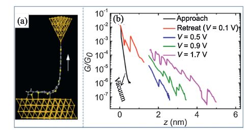
For isolated polymer chains on metal substrates,scanning tunnel microscope (STM) can pick up a single chain with tip,forming a metal/single chain/metal junction.n a pioneering experiment,Grill et al. [24] manipulated long polyfluorene chains (typically0 nm long) on Au(111) (Fig. 4a and d(1)). STM tip was first brought into close proximity to one end of a selected chain to form electronic contact,and then the chain could be lift up by retracting tip progressively. Note that the polymers could also be picked up from other points besides the ends of chains,but with lower success rates. Successful formation of polymer junction was confirmed by considerably higher current signal than vacuum tunneling (Fig. 4b) and conformation/location change of the manipulated polymer (Fig. 4c).ue to the stronger tiπ-molecule interaction than the chain-substrate interaction,polymer chain is mobilizable on surface and keeps attached to the tip during the pulling process.herefore,STM pulling enables the conductance measurement of single CPs as a continuous function of its length. Another advantage of STM is that it allows the combination of conductance measurement with imaging. Using this technique,single chains of polythiophene (Fig. 4d,reaction) [25, 26],a (donor-acceptor-donor)n type copolymer (Fig. 4d,reaction 3) [27] and graphene nanoribbon (Fig. 4d,reaction 4) [28] have also been investigated.hese CPs were all prepared by on-surface Ullmann coupling (Fig. 4d),in which aryl-halogens are thermally activated and form aryl-aryl bonds under the catalysis of metal substrates.n addition to the reactions shown in Fig. 4d,Ullmann coupling with other monomers [29-32] and substrates [30, 31],Wanzlick carbene dimerization [33],Glaser coupling [34] and Schiff-base condensation [35, 36] were also exploited to produce isolated CP chains on metallic surface and they should also be applicable to STM pulling studies.

|
Download:
|
| Figure 4. (a-c) Single-chain junction with STM manipulation [24]: (a) Schematic representation of the junction formed by STM tip, single-chain polyfluorene and metal substrate; (b) Tunneling current as a function of the tip height through vacuum and polymer chain (inset: circuit diagram of electron transport path in single-chain junction); (c) STM images showing conformation change and displacement of a polyfluorene chain after tip manipulation. (d) On-surface Ullmann coupling reactions to synthesize isolated chains for building STM pulling junctions. (a-c) Adapted with permission from [24]. Copyright 2009 AAAS. | |
2.3. Monolayered CP junctions
In nanogap junctions only a small amount of molecules are sandwiched due to the limited electrode areas.n comparison,molecular monolayers formed on substrates generally cover a large area,which lead to more robust and reproducible junctions [37]. Because of the long dimension,CPs are not amenable to form standard self-assembled monolayers (SAMs) in which molecules stand vertically on surface.n this regard,stepwise growth method has been developed to construct the “vertical” CP junctions. Besides,CP monolayers lying flat on surface have also been utilized recently to build the “planar” type junctions.
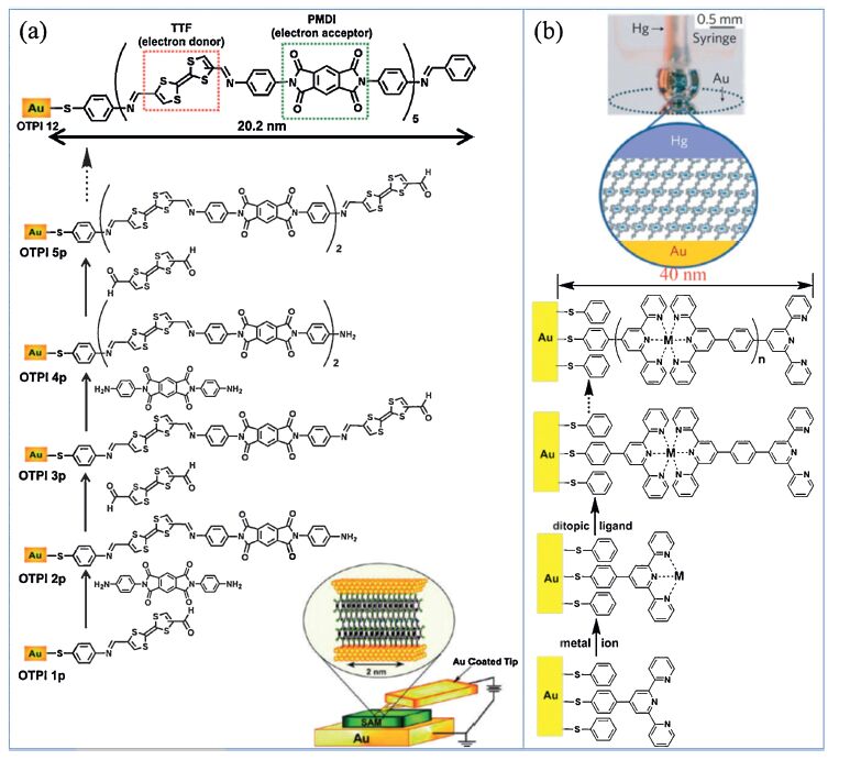
2.3.1. “Vertical” junctionsChoi andrisbie [38] prepared SAMs of CPs with length up to0 nm standing on Au surface by repetitive imine additions and built the corresponding metal/SAM/metal junction with conducting atomic force microscopy (CAFM). As shown in Fig. 5a,the stepby- step growth started from a SAM of Ar-CHO,which reacted with NH2-Ar-NH2 via imine addition; the produced aryl imines bearing -NH2 terminals were further derivatived with CHO-Ar-CHO via imine addition.ive repetitive addition steps yielded the SAM of0 nm conjugated copolymers. CP junctions were formed by bringing an Au-coated AFM tip into contact with the SAM. A junction typically incorporated ~100 CP wires in parallel,as estimated from the tip/SAM contact area of ~50 nm2. As far as we know,this is the longest conjugated wire forming junction with CAFM.

|
Download:
|
| Figure 5. Step-by-step synthetic routes for SAMs of CPs and testing methods for the metal/CPs/metal junction. (a) Repetitive imine addition steps to prepare conjugated copolymer-based SAM measured by CAFM [38]. (b) Sequential stepwise coordination to synthesize conductive polymers and SAM junctions formed with Hg-drop top contact [39]. (a) Reprinted with permission from [38]. Copyright 2010 American Chemical Society. (b) Adapted with permission from [39]. Copyright 2008 Nature Publishing Group. | |
Tuccitto et al. [39] built highly conductive coordination polymers,up to 40 nm,on metal surface and incorporated them into junction with mercury drop as top contact (Fig. 5b).he polymeric SAM was produced in situ by sequential stepwise coordination of metal ions (Fe2+ and Co2+) with terpyridine-based ligands. Mercaptobenzenes were co-assembled as lateral spacer to facilitate polymer wires stand up with highly organized structures.he junction was formed by bringing a Hg-drop electrode into contact with the SAM on Au electrode. Hg drop as top contact produced junctions with large area of ~0.15 mm2.
2.3.2. “Planar” junctionCP monolayers lying flat on electrode surface have been prepared by electrooxidation of SAMs of electro-polymerizable monomers,such as thiophene [40, 41],pyrrole [42, 43] and aniline [44]; on this basis monolayered polymer junctions can be built with CAFM [40, 43].n a study by Ocafrain et al. [40],bithiophene monomers bearing thiol groups formed SAM on Au electrode (Fig. 6a),which was subjected to recurrent potential scans in electrolyte,resulting in compact and stable polythiophene monolayer,with a thickness in the range of 16.6-19.5Å.he planar type junction was fabricated by contacting the monolayer on Au substrate with the probe of CAFM.he-V characteristics demonstrated that the CP monolayer exhibited significantly higher tunneling current than the unpolymerized SAM (Fig. 6b). Alternatively,lateral polymerization of surface-immobilized monomers was performed with scanning CAFM (Fig. 6c) [43]. Application of biases higher than ±4 V during CAFM scans induced local polymerization within the pyrrole monolayer. Such a procedure enabled the formation of polymer monolayer at desired position (Fig. 6d) and CP junctions were formed simultaneously.his technique,nevertheless,requires high density of monomers and strong chemical bondage of the monolayer to electrode surface.

|
Download:
|
| Figure 6. (a) Schematic of the electropolymerization of bithiophene SAM by potential scans [40]. (b) I-V curves of the SAM junctions before and after electropolymerization [40]. (c) Schematic of the localized electropolymerization of pyrrole using a scanning CAFM tip [43]. (d) Patterns of polypyrrole monolayer formed by localized electropolymerization [43]. (a) and (b) Adapted with permission from [40]. Copyright 2008 Wiley-VCH. (c) and (d) Reprinted with permission from [43]. Copyright 2012 American Chemical Society. | |
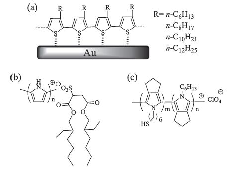
Apart from in situ polymerization on surface,CP monolayers can be obtained straightforward by assembly of as-synthesized CPs. Of particular interest is polythiophenes,which,without bearing thiols,are able to form compact and stable SAMs on Au surface through the thiophene-Au interaction [45-48],depicted in Fig. 7a. Polypyrrole,in the form of its sulfosuccinate salt,also adsorbs nicely on bare Au and Pt electrodes,due to the adsorption interaction via the sulfosuccinate moiety (Fig. 7b) [49]. Nevertheless,more general strategy for self-assembly is to endow CPs with anchoring groups,typically thiols.or example,a polypyrrole containing multiple thiol groups (Fig. 7c) has been designed to produce polypyrrole SAMs [49].or these CP monolayers,CAFM also provides a reliable technique to form junctions.n an effort to make junctions with monolayered polypyrrole (Fig. 7b and c),Vercelli et al. [49] used the plateau-style tips whose contact area was hundreds of times larger than the standard AFM tips.t is noteworthy that CPs assembled on substrates generally contain long alkyl chains.hese alkyl chains in the monolayer junction,if oriented along the charge transport direction,would probably smear the intrinsic electrical properties of conjugated backbones.

|
Download:
|
| Figure 7. Examples of CPs that can be directly assembled on electrodes in monolayer. | |
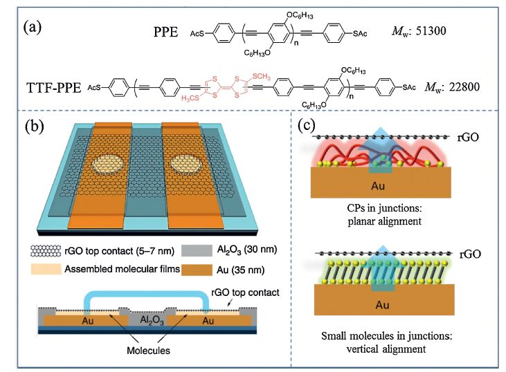
Wang et al. [50] introduced a novel molecular design strategy to assemble CPs into monolayer structure,and the junction was constructed with graphene as top contact/electrode (Fig. 8). Rather than containing multiple anchoring groups at the side chains,the CPs (i.e.,PPEs) in this work bear thiol groups only at both ends. Experimental evidences indicated that almost all the thiols had bonded to Au surface and that the long polymers were selfassembled into monolayers that lay flat on Au surface,in a distinct manner from the traditional vertically oriented small-molecule monolayers.he self-assembled PPE monolayer appeared as a continuous film with thickness of ~2 nm,comparable to that of typical small-molecule SAMs.o fabricate junctions,PPE monolayer was assembled on Au bottom electrodes in micropores,and reduced graphene oxide (rGO) films were transferred onto the molecular films to form top contact. Benefiting from the conductive and flexible graphene materials,the junctions were constructed with high device yields and operational stability; another feature is that the test bed can be performed in a doublejunction geometry,in which rGO performs as both top contacts and conductive interconnects between molecular components [51, 52].urthermore,the electronic properties of the junction were tailored by incorporating redox-active tetrathiafulvalene (TTF) units into PPE backbones.

|
Download:
|
| Figure 8. PPE-based planar junctions [50]. (a) Molecular structures of PPE and TTF-PPE. (b) Schematic view of rGO top-contact test bed. (c) Schematic view of self-assembled small molecules and long CPs inside the junctions. Adapted with permission from [50]. Copyright 2015 Nature Publishing Group. | |
3. Charge transport through CP junctions
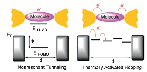
Tunneling is the principal mechanism for short-range transport.ig. 9 shows a simplified schematic view of nonresonant tunneling,in which a large energy difference exists between the molecular frontier orbitals (HOMO or LUMO) and electrodeermi level (Ef).he conductance (G) can be expressed by [2]:
| $G\propto \exp \left( \frac{-2d}{n}\sqrt{2m\Phi } \right)$ |
with d the transport distance,m the electron mass and the orbital-to-Fermi energy offset (Ef - EHOMO or Ef - ELUMO),so-called barrier height. According to this equation,the tunneling conductance decays exponentially with molecular length and depends crucially on energy offset.
n contrast,charges would “hop” between neighboring sites in multiple steps to transport over a long distance (Fig. 9) and the charge transfer is thermally activated. Hopping transport is characterized by linear length dependence of the conductance and thermal activation,following [2],
| $G\propto {{d}^{-1}}\exp \left( \frac{-{{E}_{a}}}{{{k}_{B}}T} \right)$ |

|
Download:
|
| Figure 9. Energy-diagram illustrations of nonresonant tunneling and hopping mechanisms [53]. Reprinted with permission from [53]. Copyright 2013 Royal Society of Chemistry. | |
where Ea is the Arrhenius activation energy and T is the temperature. As an example,30 nm long IMWs bridging nanogaps (see Fig. 2b) showed thermally activated charge transport,evidencing the hopping conduction [13].
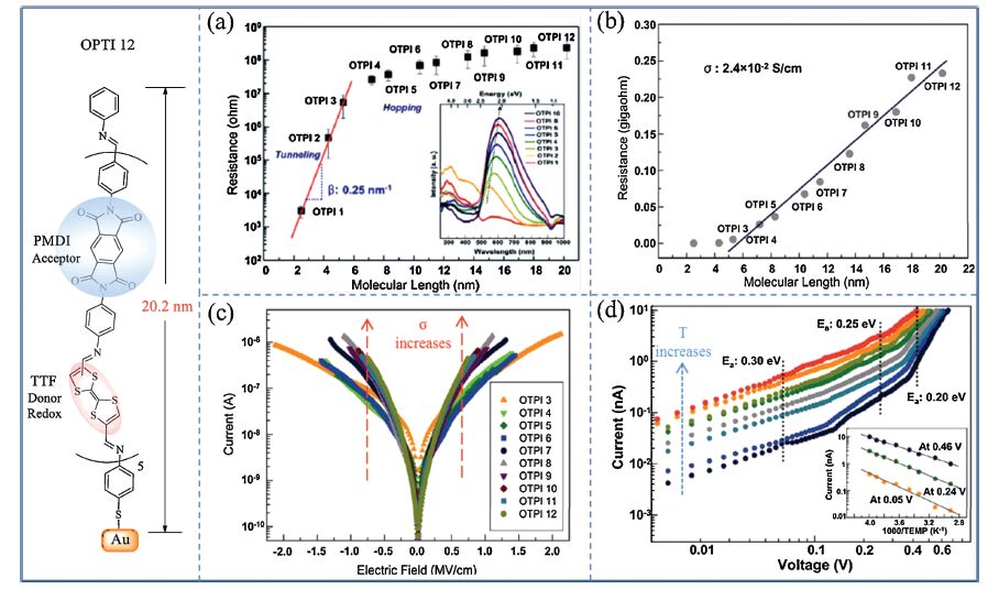
The critical length at which mechanism changes from tunneling to hopping depends on molecular structure and generally falls in the range of 3-6 nm. Choi andrisbie [38] studied OPTI molecules with length up to 0.2 nm (Fig. 10) and observed the transition at near 5 nm,as depicted in Fig. 10a.or short wires (OTPI 1-3),the resistances increased exponentially,and one can find that 3 nm length increase caused resistance 3 orders of magnitude higher.n contrast,under the hopping conduction regime (OTPI 4-12),conductance depended weakly on molecular length (linearly with a low slope),shown in Fig. 10a and b.he authors presented comprehensive investigations on length-,temperature-,and fielddependent transport behaviors of the OPTI molecules,and three results are emphasized here.Firstly,the long OPTI wires exhibited a considerably high conductivity,up to 0.024 S/cm.he high conductivity derives from the special molecular structures: (1) the donor-acceptor motif significantly lowers the optical band gap; (2) the TTF units in backbone bring multiple redox states with gap below 1.0 V,which further facilitate carrier hopping; (3) planar molecular conformation leads to extensive electronic delocalization along the conjugated wire. Secondly,the conductivity of long wires estimated from current (I)-electric filed (E) curves is higher than that of short wires at high electric fields (Fig. 10c) because of the continually increased conjugation with wire length,as evidenced by the consistent decrease in both electrochemical band gap and optical band gap with length.hirdly,the applied electric field could assist the hopping process: the larger the filed,the smaller the required thermal activation energy,disclosed from the temperature-dependent I-V characteristics for OTPI 12 (Fig. 10d).

|
Download:
|
| Figure 10. Transport properties of OPTI molecules [38]. (a) Semilog plot of resistance versus length. Inset, UV-vis absorption spectra of OTPI wires with different lengths. (b) linear plot of resistance versus length. (c) Semilog plots of current versus electric filed. (d) Temperature-dependent I-V characteristics for OTPI 12 with Arrhenius plots at different voltages (inset). Adapted with permission from [38]. Copyright 2010 American Chemical Society. | |
STM pulling technique holds the potential to investigate the length dependence of conductance of a single chain. However,in practice,the serious current decay with CP length limits the measurable length to only several nanometers in junctions [24-8].or example,above 4 nm,the current through polyfluorene chain become negligible and cannot be measured under small bias voltages [24]. Charge transport over such small distance is dominated by tunneling,and the conductance decay is quantified by attenuation factor (β),following G = Goe-βd,where Go is the contact conductance.
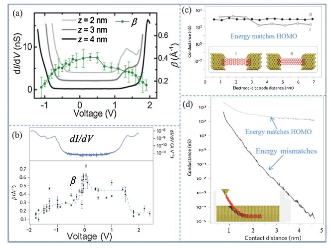
The voltage dependent transport behavior of single chain has been recognized since the first STM pulling experiment by Grill et al.,who observed increased conductance of polyfluorene at higher bias voltages [24]. Later,this phenomenon was carefully examined on graphene nanoribbon [28] and polythiophene [25, 26],by systematically measuring the current-length curves at different voltages.t was found that β became lower at higher bias values,indicating more efficient charge transport at elevated voltages. More importantly,the relatively constant β values,at low voltage region,began to decrease at the positions where electronic resonances appeared in the dI/dV spectra (Fig. 11a and b),indicating that β reduction is associated with the approaching of electron energy to molecular energy levels.n other words,the crossover from nonresonant to resonant transport takes place at higher voltages.

|
Download:
|
| Figure 11. (a) dI/dV spectra and attenuation factor as a function of voltage for polythiophene [26]. (b) dI/dV spectra and attenuation factor as a function of voltage for graphene nanoribbon [28]. (c and d) Calculated conductance of graphene nanoribbon as a function of length at different cases [28]: (c) Graphene (armchair and zigzig) with planar geometry under energy levels matched; (d) bended graphene in STM junction under energy levels matched and mismatched. (a) Reprinted with permission from [26]. Copyright 2015 American Chemical Society. (b-d) Adapted with permission from [28]. Copyright 2012 Nature Publishing Group. | |
It is also possible to achieve pseudo-ballistic charge transport when the electron energy matches HOMO or LUMO of molecules [28]. As shown in Fig. 11c,under proper bias voltage when the Fermi level of electrodes matches with the HOMO of a planar grapheme nanoribbon,its conductance keeps unchanged within a broad length range (i.e.,b = 0),revealing the pseudo-ballistic transport regime. In this case,charge transport is far more efficient than the traditional nonresonant tunneling. However,for graphene nanoribbon pulled by STM tip,even when the energy levels match each other,conductance still decays apparently (Fig. 11d),because molecular bending/deformation in the STM junction perturbs the electronic delocalization along the molecule. This result emphasizes the important influence of chain conformation on the efficient long-range charge transport.
Nacci et al. [27] proposed that alternating donor and acceptor units in backbone was a good way to enhance the charge transport ability of CP wires,considering that D-A-D is effective to lower HOMO-LUMO gap. In their work,benzobis(1,2,5-thiadiazole) units as an acceptor were doped in polythiophene chain (molecular structure is shown in Fig. 4d(3)),generating a (D-A-D)n type copolymer. This structural design gives a much smaller bandgap of 0.78 eV,in comparison with the homogeneous polythiophene with bandgap above 2 eV. The reduced energy gap improved the charge transport capability,as convinced by the low attenuation factor of 0.2Å-1 (0.4Å-1 for polythiophene). This value is also lower than that of polyfluorene (0.3Å-1) and graphene nanoribbon (0.45Å-1).
By incorporating a large number of Co (II) and Fe (II) centers into CP backbone,Tuccitto et al. [39] obtained highly conductive,extralong coordination polymers. Fig. 12a clearly shows the extremely low conductance decay with length (0.001 and 0.028Å-1),especially for Co (II) wire: 14-nm-long wires exhibited similar conductance with the 1 nmwires (i.e.,the primer for wire growth). Apparently,such surprising phenomena are associated with the disappearance of exponential decay across short wires,thus nonresonant tunneling is excluded as a transport mechanism for the short wires. In fact,the metal centers provided HOMO states that were close to electrode Fermi levels,which led to low-barrier resonant tunneling between electrodes and metal centers,and thus low current decay. On the other hand,metal centers also provided multiple redox sites,which enhanced the hopping transport along the long wires (Fig. 12b).

|
Download:
|
| Figure 12. Ultralow conductance decay of Co (II)- and Fe (II)-based coordination polymers [39]. (a) ln J versus length of the Co (II)- and Fe (II)-based wires. (b) Energy diagram and transport mechanism for junctions of the Co (II)- and Fe (II)-based wires. Adapted with permission from [39]. Copyright 2008 Nature Publishing Group. | |
Conductance decay with length is the underlying principle limiting the long-range transport capability of long molecules,e.g.,CPs. Considering the serious decay in tunneling transport and shallow decay in hopping transport,one can easily identify that high β value during tunneling is the bottleneck in achieving high conductance of long wires. According to the Simmons model,β mainly depends on barrier height,described as follows [54]:
| $\beta =\frac{2a\sqrt{2m\Phi }}{n}$ |
where a is a unitless parameter that is introduced to modify the simple rectangular barrier model or to account for an effective mass. Therefore,bringing molecular frontier orbitals close to Fermi level is expected to obtain low β values. In particular,when Fermi energies are resonant with HOMO or LUMO,charges are injected directly into molecules without barrier,i.e.,resonant tunneling takes place. To reduce the energy offset,two viable strategies have been exploited [39]: providing energy states close to Fermi level by incorporating metal redox centers into backbone,and lowering HOMO-LUMO energy gap by extending π-delocalization length.Over the past decade,ultralow attenuation (β < 0.1Å-1) has been realized in a few molecular systems,as presented in Fig. 13. These molecules typically possess multiple metal redox centers,highdegree of electronic delocalization,rigid backbones,low bandgaps and small energy offsets [39, 55-63]. These ultralow β values suggest that CPs would be able to mediate long-range charge transport with very slow conductance decay with length,if their molecular and electronic structures are properly designed. It is very likely that such kind of CPs could be developed by elongation of the oligomers shown in Fig. 13. In addition,theory calculations have predicted some highly conductive polymer chains. For example,density functional theory calculations revealed that highly flexible multidecker bis(benzene)chromium wires might have ultralow β values (0.068-0.079Å-1) and their conductance keeps relatively unaffected even they are twisted and coiled [64]. It is also interesting to see that MMX [Pt2(CH3CS2)4I]n polymer chain exhibits metallic behavior rather than traditional semiconducting state [65].

|
Download:
|
| Figure 13. Ultralow β values reported for molecules: 1 [55],2a [39],2b [39, 56],3 [57],4a [58],4b [59],5 [60, 61],6 [62],7 [63]. | |
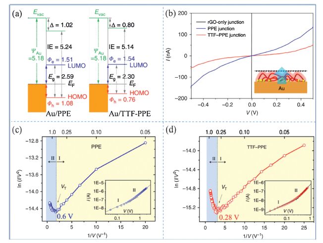
For CP monolayers that are lying flat on electrode,the thickness of the molecular layer is generally less than 3 nm [40, 43, 47, 49, 50],thus transport through the planar junctions can be described by tunneling [50]. Molecular-specific transport characteristics of CP monolayers have been reported in such tunneling junctions (Fig. 14) [50]. By incorporating TTF into PPE backbone,Ef - EHOMO HOMO energy barrier was effectively lowered (Fig. 14a),revealed by XPS and UPS characterizations. On the other hand,transition voltage spectroscopy,derived from I-V data (Fig. 14b),showed evidently smaller transition voltage of TTF-PPE junction (Fig. 14c and d),indicating smaller charge injection barriers in the case of TTF-PPE. Therefore,electrical measurements gave result that was consistent with spectroscopic characterizations. The molecularspecific characteristics revealed in the monolayer tunneling junction opens a way for employing tailor-made polymeric components as alternatives to small molecules for molecularscale electronic devices [50].

|
Download:
|
| Figure 14. Molecular-specific characteristics of monolayer tunneling junctions [50]. (a) Representative I-V curves of rGO-only junctions and junctions based on PPE and TTF-PPE monolayer. (b) Energy level diagrams of Au/PPE and Au/TTF-PPE. (c and d) Fowler-Nordheim plots for I-V traces of junctions based on PPE (c) and TTF-PPE (d). Adapted with permission from [50]. Copyright 2015 Nature Publishing Group. | |
The conductance of single-chain CP is strongly affected by mechanical stress,which has been carefully studied using STM pulling experiments (Fig. 15) [26]. During polythiophene being pulled by a tip,stress was applied on the suspended chain,which affected the molecular orbits,reduced the conjugated degree and weakened the coupling at chain/tip interface accompanied with longer Au-C bond. Once the accumulated stress was released,as a thiophene subunit detached from Au surface,the current traversing the junction increased abruptly (Fig. 15b),resulting from conjugation gain and better coupling with electrodes. The increase overwhelmed the expected exponential decrease of the conductance with molecular length. Note that the strong conductance jump was not observed for polyfluorene [24] or graphene nanoribbon [28],probably because adsorption of them on Au substrate is too weak to accumulate much stress that affects the conductance [26]. This experiment suggests the possibility of regulating the transport properties of molecular junctions by mechanical means.

|
Download:
|
| Figure 15. Conductance changes related to mechanical stress. (a) Schematic representation of polythiophene junction, which clearly shows the adsorption interaction of thiophene rings with Au substrate [26]. (b) Abrupt conductance changes during tip pulling [25]. (a) Reprinted with permission from [26]. Copyright 2015 American Chemical Society. (b) Reprinted with permission from [25]. Copyright 2014 American Physical Society. | |
The differences in charge transport behavior between singlechain CPs and CPs at larger scales have been explored. PPE single chain (18 nm long) behaved like a quantum transport device,as indicated by the I-V curve that exhibited stepwise features with period of 0.23-0.26 V [15],while PPE nanowire (20 nm in diameter) displayed stepwise characteristics with much larger step interval of 1 V [66]. The telegraphic conductance switching phenomenon of single-chain polyaniline was observed [12],which was significantly distinct from the conductance behaviors of single-nanocrystalline-domain polyaniline and bulk polyaniline [67].
4. Potential applicationsCPs features long dimension and electrical conductivity,which make them a promising kind of molecular wires. Moreover,outstanding optoelectronic properties and structural functionalizations are expected to endow CPs with desired electronic functions.
4.1. Molecular wireOne of the goals of molecular electronics is to integrate various functional elements using molecular wires. A molecular wire should be conductive enough for electronic communication,must ensure stable bonding to functional molecules and needs to be created at designated positions [68]. CPs potentially meet these requirements. Okawa et al. [68] developed a “chemical soldering” method,using conductive polydiacetylene (PDA) wires to connect functional molecules at designated positions. As shown in Fig. 16a,diacetylene molecules formed a SAM,and STM tip initiated the chain polymerization in SAM to produce conductive PDA wires; during the chain propagation,the reactive carbenes at chain ends reacted with the functional molecule to form covalent bonds. Fig. 16b shows phthalocyanine (Pc) pentamer absorbed on the SAM was connected with a PDA chain on one side,and it was further connected by a second PDA chain from the other side (Fig. 16c). The authors further showed that the produced PDA-ZnPc-PDA structure could act as a molecular resonant tunneling diode (Fig. 16d),a useful component of single-molecule electronics. Fullerene has also been connected with PDA wires using this soldering technique [69].

|
Download:
|
| Figure 16. Chemical soldering with PDA [68]. (a) Schematic illustration of chemical soldering. (b) STM image showing single PDA wire connected to a Pc molecule. (c) STM image showing two PDA wires connected to a Pc molecule. (d) Energy level diagram of a PDA-ZnPc-PDA system and expected application as a molecular resonant-tunneling diode. Adapted with permission from [68]. Copyright 2011 American Chemical Society. | |
4.2. Molecular switch
By linking photochromic diarylethene (which undergoes reversible ring-opening and ring-closed state under UV and visible light,respectively) into IMW backbone (Fig. 2b),the corresponding CP junction displayed higher conductance once illuminated with UV light but lower conductance under visible light,with an on-off ratio of 20 (Fig. 17a) [13].

|
Download:
|
| Figure 17. Polymer switches. (a) Photoswitching behavior of diarylethene-containing CP wires [13]. (b) A photo-responsive molecular wires composed of porphyrin polymer and fullerenes [14]. (c) Photoresponse characteristics of PPE junction [70]. (d) Conductance switching of TTF-PPE junction under large applied bias sweeps [50]. (a) Adapted with permission from [13]. Copyright 2006 American Chemical Society. (b) Reprinted with permission from [14]. Copyright 2009 Royal Society of Chemistry. (c) Reprinted with permission from [70]. Copyright 2005 American Chemical Society. (d) Adapted with permission from [50]. Copyright 2015 Nature Publishing Group. | |
Fullerenes were decorated onto porphyrin polymer chain to develop a photo-responsive molecular wire (Fig. 2c) [14]. As shown in Fig. 17b,the photo-switching behavior derives from the photoexcited electron transfer from porphyrin to fullerene; the holes in excited porphyrins lead to increased conductivity,as compared to the neutral porphyrins. In the CP junction,1-4-fold higher conductivity was observed under light than in the dark,depending on the temperature. The photoexcitation-induced conductance switch was also observed in self-assembled PPE junction [70]. Significantly,the speed of photoresponsewas very fast,with frequency of 400 Hz,and the switching ratio was as high as 1000 (Fig. 17c).
By incorporating redox-active TTF units in PPE backbones (Fig. 8a),monolayered CP junction was endowed with redoxswitching functionality [50]. In solution,TTF-PPEs can be reversibly oxidized/reduced by CV methods. This principle was applied to the solid-state CP junction. Fig. 17d clearly shows the conductance switching characteristics of TTF-PPE junction under large bias sweeps,confirming that the redox states can be reversibly tuned in solid junctions by applying voltages. Regarding the redox switching in molecular devices,electrochemical method holds advantages over using chemicals.
4.3. Molecular rectifierVercelli et al. [49] observed rectification behaviors in monolayered polypyrrole planar junctions (molecular structure shown in Fig. 18a). As displayed in Fig. 18b,Au/PPy/Au junction exhibited asymmetric I-V characteristic,which fit well to Schottky equation. The rectification ratio was significantly high,up to 150 at 0.5 V. It is noteworthy that,the classical donor-acceptor structure for rectification does not exist in this polymer,but it actually rectifies current. This phenomenon was ascribed to the asymmetrical arrangement of polypyrrole chains in the junction,resulting from their interactions with long alkyl sulfonate,i.e.,sulfosuccinate. This interpretation could be supported by the fact that rectification was quenched once adding a layer of Nafion (Fig. 18c),also a kind of long alkyl sulfonate,which should be able to balance the polypyrrole chains in junction. Interestingly,inverting the bilayer sequence into Au/Nafion/PPy/Au structure,the junction also presented rectifying effect (Fig. 18d),with rectification ratio of 10. This work demonstrates the potential of monolayered CPs in achieving high-performance molecular rectifier. It also implies that,for multilayered polymer junction,rectification can be optimized by changing the sequence of monolayer materials.

|
Download:
|
| Figure 18. Molecular rectifiers based on CP monolayer [49]. (a) Molecular structure of the CP for construction molecular rectifier. (b-d) I-V plots for the junctions of Au/PPy/Au (b), Au/PPy/Nafion/Au (c) and Au/Nafion/PPy/Au (d). Adapted with permission from [49]. Copyright 2006 American Chemical Society. | |
4.4. Light-emitting diode
The first single-molecule light-emitting diode (LED) was developed with single-chain polythiophene (Fig. 19) [25]. Polythiophene wire emitted red light when biased positively (e.g. 2 V) in the STM junction and the emission wavelength did not shift with higher voltages (Fig. 19b),whereas the electroluminescence was negligible at the negative bias. The electroluminescence follows the classical emission mechanism,in which electrons injected from the tip in LUMO recombines holes in HOMO of the molecule (Fig. 19c). LED behavior was brought from the specific electronic structure of the polymer junction,i.e.,the asymmetric alignment of the polymer HOMO-LUMO gap with respect to electrode EF at V = 0 and the asymmetric voltage drop repartition at the polymer/ electrode interfaces (Fig. 19c). Moreover,the electroluminescent properties were affected by polymer conformation,orbital bandwidth and plasmons at STM junction. This work paves the way toward miniaturization of LEDs at the single-molecule scale.

|
Download:
|
| Figure 19. Single-chain polythiophene LED [25]. (a) Artistic view of fluorescent polythiophene junction. (b) Light emission spectra as a function of the applied voltage. (c) Energy-level model showing the electronic structure and the emission mechanism of the junction. Adapted with permission from [25]. Copyright 2014 American Physical Society. | |
5. Conclusion and perspective
In this review,we have shown that conjugated polymers are emerging as potential candidates for molecular electronics,as an alternative to the extensively studied small-molecule systems. Polymer junctions have been fabricated to work in the manners where charges transport along the long individual CP chains or tunneling across a flat-lying monolayer. CP chains are able to mediate long-range charge transport with very slow conductance decay with length if polymer structures are properly designed. Single-chain and monolayered CPs have demonstrated their promising applications in molecular wire,molecular switch,molecular rectifier and light-emitting diode.
Controlled incorporation of single-chain and monolayered CPs into molecular junctions still remains as the primary challenge,which calls for multi-disciplinary efforts from physicists,chemists,nanoscientists,etc. Moreover,charge transport properties of CPs at the single-molecule level remain largely unexplored,and the establishment of structure-transport-function relationships will be a long-term task. Hopefully the investigations on CP-based molecular electronics will eventually lead to the development of electronic devices with superior performance and will improve our understanding on the structure-property relationships of single molecules at long dimensions.
Acknowledgments The authors acknowledge the financial support from 985/211 Project (No. WF220411002), Shanghai Jiao Tong University and the national "1000-talent Plan (Youth)".| [1] | D. Xiang, X. Wang, C. Jia, et al. Molecular-scale electronics: from concept to function. Chem. Rev. 116 (2016) 4318–4440. DOI:10.1021/acs.chemrev.5b00680 |
| [2] | R.M. Metzger. Unimolecular electronics. Chem. Rev. 115 (2015) 5056–5115. DOI:10.1021/cr500459d |
| [3] | B. Mann. Tunneling through fatty acid salt monolayers. J. Appl. Phys. 42 (1971) 4398–4405. DOI:10.1063/1.1659785 |
| [4] | A. Aviram, M.A. Ratner. Molecular rectifiers. Chem. Phys. Lett. 29 (1974) 277–283. DOI:10.1016/0009-2614(74)85031-1 |
| [5] | L. Sun, Y.A. Diaz-Fernandez, T.A. Gschneidtner, et al. Single-molecule electronics: from chemical design to functional devices. Chem. Soc. Rev. 43 (2014) 7378–7411. DOI:10.1039/C4CS00143E |
| [6] | A. Facchetti. p-Conjugated polymers for organic electronics and photovoltaic cell applications. Chem. Mater. 23 (2011) 733–758. DOI:10.1021/cm102419z |
| [7] | L. Luo, S.H. Choi, C.D. Frisbie. Probing hopping conduction in conjugated molecular wires connected to metal electrodes. Chem. Mater. 23 (2011) 631–645. DOI:10.1021/cm102402t |
| [8] | H. Yan, A.J. Bergren, R. McCreery, et al. Activationless charge transport across 4.5 to 22 nm in molecular electronic junctions. Proc. Natl. Acad. Sci. U.S.A. 110 (2013) 5326–5330. DOI:10.1073/pnas.1221643110 |
| [9] | H. Liu, N. Wang, J. Zhao, et al. Length-dependent conductance of molecular wires and contact resistance in metal-molecule-metal junctions. ChemPhysChem 9 (2008) 1416–1424. DOI:10.1002/cphc.v9:10 |
| [10] | S.H. Choi, B. Kim, C.D. Frisbie. Electrical resistance of long conjugated molecular wires. Science 320 (2008) 1482–1486. DOI:10.1126/science.1156538 |
| [11] | T. Li, W. Hu, D. Zhu. Nanogap electrodes. Adv. Mater. 22 (2010) 286–300. DOI:10.1002/adma.v22:2 |
| [12] | H.X. He, X.L. Li, N.J. Tao, et al. Discrete conductance switching in conducting polymer wires. Phys. Rev. B 68 (2003) 045302. DOI:10.1103/PhysRevB.68.045302 |
| [13] | M. Taniguchi, Y. Nojima, K. Yokota, et al. Self-organized interconnect method for molecular devices. J. Am. Chem. Soc. 128 (2006) 15062–15063. DOI:10.1021/ja065806z |
| [14] | H. Ozawa, M. Kawao, S. Uno, et al. A photo-responsive molecular wire composed of a porphyrin polymer and a fullerene derivative. J. Mater. Chem. 19 (2009) 8307–8313. DOI:10.1039/b910638c |
| [15] | W.P. Hu, J. Jiang, H. Nakashima, et al. Electron transport in self-assembled polymer molecular junctions. Phys. Rev. Lett. 96 (2006) 027801. DOI:10.1103/PhysRevLett.96.027801 |
| [16] | M.J. Frampton, H.L. Anderson. Insulated molecular wires. Angew. Chem. Int. Ed. 46 (2007) 1028–1064. DOI:10.1002/(ISSN)1521-3773 |
| [17] | C. Pan, C. Zhao, M. Takeuchi, et al. Conjugated oligomers and polymers sheathed with designer side chains. Chem. Asian J. 10 (2015) 1820–1835. DOI:10.1002/asia.201500452 |
| [18] | J. Terao, Y. Tsuji. New synthetic methods of p-conjugated inclusion complexes with high conductivity. J. Incl. Phenom. Macrocycl. Chem. 80 (2014) 165–175. DOI:10.1007/s10847-014-0381-y |
| [19] | T. Shimomura, T. Akai, T. Abe, et al. Atomic force microscopy observation of insulated molecular wire formed by conducting polymer and molecular nanotube. J. Chem. Phys. 116 (2002) 1753–1756. DOI:10.1063/1.1446423 |
| [20] | J.S. Wilson, M.J. Frampton, J.J. Michels, et al. Supramolecular complexes of conjugated polyelectrolytes with poly(ethylene oxide): multifunctional luminescent semiconductors exhibiting electronic and ionic transport. Adv. Mater. 17 (2005) 2659–2663. DOI:10.1002/(ISSN)1521-4095 |
| [21] | J. Terao, Y. Tanaka, S. Tsuda, et al. Insulated molecular wire with highly conductive π-conjugated polymer core. J. Am. Chem. Soc. 131 (2009) 18046–18047. DOI:10.1021/ja908783f |
| [22] | H. Masai, J. Terao, S. Seki, et al. Synthesis of one-dimensional metal-containing insulated molecular wire with versatile properties directed toward molecular electronics materials. J. Am. Chem. Soc. 136 (2014) 1742–1745. DOI:10.1021/ja411665k |
| [23] | T. Shimomura, T. Akai, M. Fujimori, et al. Conductivity measurement of insulated molecular wire formed by molecular nanotube and polyaniline. Synth. Met. 153 (2005) 497–500. DOI:10.1016/j.synthmet.2005.07.305 |
| [24] | L. Lafferentz, F. Ample, H. Yu, et al. Conductance of a single conjugated polymer as a continuous function of its length. Science 323 (2009) 1193–1197. DOI:10.1126/science.1168255 |
| [25] | G. Reecht, F. Scheurer, V. Speisser, et al. Electroluminescence of a polythiophene molecular wire suspended between a metallic surface and the tip of a scanning tunneling microscope. Phys. Rev. Lett. 112 (2014) 047403. DOI:10.1103/PhysRevLett.112.047403 |
| [26] | G. Reecht, H. Bulou, F. Scheurer, et al. Pulling and stretching a molecular wire to tune its conductance. J. Phys. Chem. Lett. 6 (2015) 2987–2992. DOI:10.1021/acs.jpclett.5b01283 |
| [27] | C. Nacci, F. Ample, D. Bleger, et al. Conductance of a single flexible molecular wire composed of alternating donor and acceptor units. Nat. Commun. 6 (2015) 7397. DOI:10.1038/ncomms8397 |
| [28] | M. Koch, F. Ample, C. Joachim, et al. Voltage-dependent conductance of a single graphene nanoribbon. Nat. Nanotechnol. 7 (2012) 713–717. DOI:10.1038/nnano.2012.169 |
| [29] | L. Lafferentz, V. Eberhardt, C. Dri, et al. Controlling on-surface polymerization by hierarchical and substrate-directed growth. Nat. Chem. 4 (2012) 215–220. DOI:10.1038/nchem.1242 |
| [30] | J.A. Lipton-Duffin, J.A. Miwa, M. Kondratenko, et al. Step-by-step growth of epitaxially aligned polythiophene by surface-confined reaction. Proc. Natl. Acad. Sci. U.S.A. 107 (2010) 11200–11204. DOI:10.1073/pnas.1000726107 |
| [31] | J.A. Lipton-Duffin, O. Ivasenko, D.F. Perepichka, et al. Synthesis of polyphenylene molecular wires by surface-confined polymerization. Small 5 (2009) 592–597. DOI:10.1002/smll.v5:5 |
| [32] | L. Grill, M. Dyer, L. Lafferentz, et al. Nano-architectures by covalent assembly of molecular building blocks. Nat. Nanotechnol. 2 (2007) 687–691. DOI:10.1038/nnano.2007.346 |
| [33] | M. Matena, T. Riehm, M. Stöhr, et al. Transforming surface coordination polymers into covalent surface polymers: linked polycondensed aromatics through oligomerization of N-heterocyclic carbene intermediates. Angew. Chem. Int. Ed. 47 (2008) 2414–2417. DOI:10.1002/(ISSN)1521-3773 |
| [34] | B. Cirera, Y. Zhang, J. Björk, et al. Synthesis of extended graphdiyne wires by vicinal surface templating. Nano Lett. 14 (2014) 1891–1897. DOI:10.1021/nl4046747 |
| [35] | X.H. Liu, C.Z. Guan, Q.N. Zheng, et al. Molecular engineering of Schiff-base linked covalent polymers with diverse topologies by gas-solid interface reaction. J. Chem. Phys. 142 (2015) 101905. DOI:10.1063/1.4906271 |
| [36] | Z. Gong, B. Yang, H. Lin, et al. Structural variation in surface-supported synthesis by adjusting the stoichiometric ratio of the reactants. ACS Nano 10 (2016) 4228–4235. DOI:10.1021/acsnano.5b07601 |
| [37] | R.L. McCreery, A.J. Bergren. Progress with molecular electronic junctions: meeting experimental challenges in design and fabrication. Adv. Mater. 21 (2009) 4303–4322. DOI:10.1002/adma.v21:43 |
| [38] | S.H. Choi, C.D. Frisbie. Enhanced hopping conductivity in low band gap donoracceptor molecular wires up to 20 nm in length. J. Am. Chem. Soc. 132 (2010) 16191–16201. DOI:10.1021/ja1060142 |
| [39] | N. Tuccitto, V. Ferri, M. Cavazzini, et al. Highly conductive 40-nm-long molecular wires assembled by stepwise incorporation of metal centres. Nat. Mater. 8 (2008) 41–46. |
| [40] | M. Oçafrain, T.K. Tran, P. Blanchard, et al. Electropolymerized self-assembled monolayers of a 3,4-ethylenedioxythiophene-thiophene hybrid system. Adv. Funct. Mater. 18 (2008) 2163–2171. DOI:10.1002/adfm.v18:15 |
| [41] | A. Berlin, G. Zotti, G. Schiavon, et al. Adsorption of carboxyl-terminated dithiophene and terthiophene molecules on ITO electrodes and their electrochemical coupling to polymer layers. The influence of molecular geometry. J. Am. Chem. Soc. 120 (1998) 13453–13460. DOI:10.1021/ja9824728 |
| [42] | R.L. McCarley, R.J. Willicut. Tethered monolayers of poly((N-pyrrolyl)alkanethiol) on Au. J. Am. Chem. Soc. 120 (1998) 9296–9304. DOI:10.1021/ja981677d |
| [43] | J.S. Lee, Y.S. Chi, I.S. Choi, et al. Local scanning probe polymerization of an organic monolayer covalently grafted on silicon. Langmuir 28 (2012) 14496–14501. DOI:10.1021/la302526t |
| [44] | S. Kuwabata, R. Fukuzaki, M. Nishizawa, et al. Electrochemical formation of a polyaniline-analogue monolayer on a gold electrode. Langmuir 15 (1999) 6807–6812. DOI:10.1021/la981719b |
| [45] | Z. Gao, S.S. Kok, S.O.C. Hardy. Self-assembled conducting polymer monolayers of poly(3-octylthiophene) on gold electrodes. Synth. Met. 75 (1995) 5–10. DOI:10.1016/0379-6779(95)03384-V |
| [46] | Z. Gao, K.S. Siow. Ultramicroelectrode ensembles based on self-assembled polymeric monolayers on gold electrodes. Electrochim. Acta 42 (1997) 315–321. DOI:10.1016/0013-4686(96)00187-9 |
| [47] | D. Yang, M. Zi, B. Chen, et al. Separation of pinhole and tunneling electron transfer processes at self-assembled polymeric monolayers on gold electrodes. J. Electroanal. Chem. 470 (1999) 114–119. DOI:10.1016/S0022-0728(99)00216-8 |
| [48] | Y. Shimoyama. Growth process of poly (3-dodecyl thiophene) self-assembled monolayers: FTIR-RAS and gravimetric studies. Thin Solid Films (2004) 403-407–464-465. |
| [49] | B. Vercelli, G. Zotti, A. Berlin, et al. Polypyrrole self-assembled monolayers and electrostatically assembled multilayers on gold and platinum electrodes for molecular junctions. Chem. Mater. 18 (2006) 3754–3763. DOI:10.1021/cm060802e |
| [50] | Z. Wang, H. Dong, T. Li, et al. Role of redox centre in charge transport investigated by novel self-assembled conjugated polymer molecular junctions. Nat. Commun. 6 (2015) 7478. DOI:10.1038/ncomms8478 |
| [51] | T. Li, J.R. Hauptmann, Z. Wei, et al. Solution-processed ultrathin chemically derived graphene films as soft top contacts for solid-state molecular electronic junctions. Adv. Mater. 24 (2012) 1333–1339. DOI:10.1002/adma.201104550 |
| [52] | T. Li, M. Jevric, J.R. Hauptmann, et al. Ultrathin reduced graphene oxide films as transparent Top-Contacts for light switchable solid-state molecular junctions. Adv. Mater. 25 (2013) 4164–4170. DOI:10.1002/adma.201300607 |
| [53] | S. Rigaut. Metal complexes in molecular junctions. Dalton Trans. 42 (2013) 15859–15863. DOI:10.1039/c3dt51487k |
| [54] | W.Y. Wang, T. Lee, M.A. Reed. Mechanism of electron conduction in self-assembled alkanethiol monolayer devices. Phys. Rev. B 68 (2003) 21–35. |
| [55] | B.S. Kim, J.M. Beebe, C. Olivier, et al. Temperature and length dependence of charge transport in redox-active molecular wires incorporating ruthenium(II) bis(s-arylacetylide) complexes. J. Phys. Chem. C 111 (2007) 7521–7526. DOI:10.1021/jp068824b |
| [56] | C. Musumeci, G. Zappalà, N. Martsinovich, et al. Nanoscale electrical investigation of layer-by-layer grown molecular wires. Adv. Mater. 26 (2014) 1688–1693. DOI:10.1002/adma.201304848 |
| [57] | V. Kolivoška, M. Valášek, M. Gál, et al. Single-molecule conductance in a series of extended viologen molecules. J. Phys. Chem. Lett. 4 (2013) 589–595. DOI:10.1021/jz302057m |
| [58] | G. Sedghi, K. Sawada, L.J. Esdaile, et al. Single molecule conductance of porphyrin wires with ultralow attenuation. J. Am. Chem. Soc. 130 (2008) 8582–8583. DOI:10.1021/ja802281c |
| [59] | G. Sedghi, V.M. García-Suárez, L.J. Esdaile, et al. Long-range electron tunnelling in oligo-porphyrin molecular wires. Nat. Nanotechnol. 6 (2011) 517–523. DOI:10.1038/nnano.2011.111 |
| [60] | Z. Li, T. Park, J. Rawson, et al. Quasi-ohmic single molecule charge transport through highly conjugated meso-to-meso ethyne-bridged porphyrin wires. Nano Lett. 12 (2012) 2722–2727. DOI:10.1021/nl2043216 |
| [61] | R.C. Bruce, R. Wang, J. Rawson, et al. Valence band dependent charge transport in bulk molecular electronic devices incorporating highly conjugated multi-. J. Am. Chem. Soc. 138 (2016) 2078–2081. DOI:10.1021/jacs.5b10772 |
| [62] | G. Sedghi, L.J. Esdaile, H.L. Anderson, et al. Comparison of the conductance of three types of porphyrin-based molecular wires: b,meso, b-fused tapes, mesobutadiyne-linked and twisted meso-meso linked oligomers. Adv. Mater. 24 (2012) 653–657. DOI:10.1002/adma.201103109 |
| [63] | Q. Ferreira, A.M. Bragança, L. Alcácer, et al. Conductance of well-defined porphyrin self-assembled molecular wires up to 14 nm in length. J. Phys. Chem. C 118 (2014) 7229–7234. DOI:10.1021/jp501122n |
| [64] | J. Jiang, J.R. Smith, Y. Luo, et al. Multidecker bis(benzene)chromium: opportunities for design of rigid and highly flexible molecular wires. J. Phys. Chem. C 115 (2011) 785–790. DOI:10.1021/jp109782q |
| [65] | A. Calzolari, S.S. Alexandre, F. Zamora, et al. Metallicity in individual MMX chains. J. Am. Chem. Soc. 130 (2008) 5552–5562. DOI:10.1021/ja800358c |
| [66] | W. Hu, H. Nakashima, K. Furukawa, et al. Self-assembled rigid conjugated polymer nanojunction and its nonlinear current-voltage characteristics at room temperature. Appl. Phys. Lett. 85 (2004) 115–157. DOI:10.1063/1.1769590 |
| [67] | H. He, J. Zhu, N.J. Tao, et al. A conducting polymer nanojunction switch. J. Am. Chem. Soc. 123 (2001) 7730–7731. DOI:10.1021/ja016264i |
| [68] | Y. Okawa, S.K. Mandal, C. Hu, et al. Chemical wiring and soldering toward allmolecule electronic circuitry. J. Am. Chem. Soc. 133 (2011) 8227–8233. DOI:10.1021/ja111673x |
| [69] | M. Nakaya, Y. Okawa, C. Joachim, et al. Nanojunction between fullerene and onedimensional conductive polymer on solid surfaces. ACS Nano 8 (2014) 12259–12264. DOI:10.1021/nn504275b |
| [70] | W. Hu, H. Nakashima, K. Furukawa, et al. A self-assembled nano optical switch and transistor based on a rigid conjugated polymer, thioacetyl-end-functionalized poly(para-phenylene ethynylene). J. Am. Chem. Soc. 127 (2005) 2804–2805. DOI:10.1021/ja0433929 |