 2016, Vol.27


Over the past decades, organic semiconductors in field-effect transistors (FETs) have attracted great attention for their low-cost, flexible and large-area electronic applications such as memory devices [1, 2], displays [3] and sensors [4]. Nowadays great achievements in FETs have been obtained based on small molecules and polymers through molecular design and device optimization [5, 6, 7, 8, 9, 10, 11, 12, 13, 14, 15, 16]. Among organic semiconductors, diketopyrrolopyrroles (DPP)-based small molecules and polymers have aroused significant concern due to their promising application in organic FETs [17, 18, 19]. Experimentally, DPP-based polymer semiconductors show amazing performance. Liu et al. combined a highly-extended (E)-2-(2-(thiophen-2-yl)vinyl)thiophene (TVT) unit with the dithienyl-DPP unit, the co-polymer exhibited a high hole mobility up to 8.2 cm2 V-1 s-1 [20]. Lee et al. have developed a dithienyl-diketopyrrolopyrrole (TDPP) and selenophene containing polymer with hybrid siloxane-solubilizing groups (PTDPPSe-Si) [21]. After tuning the alkyl spacer length of the hybrid side chains, high hole and electron mobilities up to 8.84 and 4.34 cm2 V-1 s-1 have been obtained [22]. Li et al. developed a very high molecularweight DPP-DTT-based polymer, which exhibited a very high mobility up to 10.5 cm2 V-1 s-1 in organic thin-film transistor (OTFT) devices [23]. Kim et al. investigated the relationship between molecular structure and electrical properties, and obtained remarkably high hole mobility up to 13.9 cm2 V-1 s-1 [24]. Besides, DPP based polymers showed good performance in electron transport as well. Li et al. added two 1-pyridinyl groups onto DPP core to alleviate steric interaction with the DPP core, and obtained the ambipolar performance with a high electron mobility value of 6.3 cm2 V-1 s-1 in OTFT devices [25]. Kwon et al. reported impressively high electron mobility up to 7.0 cm2 V-1 s-1 in polymer OFETs by introducing one nitrile group to the vinylene moiety to obtain PDPP-CNTVT [26]. Although great achievements have been made in DPP-based polymers, the performance of DPPbased small molecules is much lower. Currently, DPP-based small molecules exhibit the highest hole mobility of 0.7 cm2 V-1 s-1 in thin films prepared by vacuum deposition [27] and the highest electron mobility of 0.96 cm2 V-1 s-1 in crystals formed through the solvent-vapor evaporation crystal growth method [28]. The discrepancy between the DPP-based polymers and small molecules spurs investigation on the reason(s) for the low performance of the small molecules.
In this work, we studied three DPP-based small molecules with different substituent, diphenyl (PDPPP), di(4-fluorophenyl) (FPDPPPF) and di(4-n-butylphenyl) (BuPDPPPBu) groups (Fig. 1), respectively. We obtained well-aligned crystals by droplet-pinned crystallization (DPC) method [11]. Careful examination on the crystalmorphologies reveals the rough and stepped crystal surfaces. FETs based on these aligned crystals showed hole mobility up to 0.19 cm2 V-1 s-1 and electron mobility up to 0.008 cm2 V-1 s-1 from PDPPP and FPDPPPF, respectively. The relatively low charge mobility is attributed to the non-intimate interface between the rough crystal surfaces and the substrate.

|
Download:
|
| Fig. 1.The structures of DPP-based small molecules. | |
PDPPP, FPDPPPF and BuPDPPPBu were synthesized according to the literature procedure and purified by chromatography on silica gel [29]. Orientated crystals were grown in situ on a piece of highly doped silicon substrate (1 cm × 1 cm) with 300 nm SiO2. Divinyltetramethyldisiloxanebis(benzocyclobutene) (BCB) (Dow Chemicals) was modified on SiO2, which was spin-coated from a mesitylene (Fluka) solution (VBCB:Vmesitylene = 1:30) and then thermally cross-linked on a hot plate in an N2 glovebox. Organic semiconductors were dissolved in para-xylene (Sigma- Aldrich) with the concentration of 0.4 μg/mL. A solution (15 mL) was dropped onto the substrate with a piece of silicon wafer (0.3 cm × 0.3 cm, pinner) to pin the solution droplet. The substrate was placed on a Teflon slide inside a Petri dish (35 mm × 10 mm) sealed with parafilm on a hotplate of 30 ± 1 ℃. After the solvent slowly evaporated, orientated crystals were formed in 30 min.
The morphology of crystals was characterized by optical microscopy (OM, Nikon LV100 POL) and atomic force microscope (AFM, Veeco). FETs were constructed in bottom-gate, top-contact configuration by depositing source and drain electrodes (80 nmAu), using a shadow mask with channel length (L) of 50 mm and width (W) of 1mm. FETs performances were measured in an N2 glovebox using a Keithley 4200-SCS semiconductor parameter analyzer. The measured capacitance of the BCB-covered SiO2/Si substrate was 10 nF cm-2 , and this value was used for mobility calculation. For statistics, data of charge mobility are presented as mean ± SD.
3. Results and discussionWe used the DPC method [11] to grow crystals of the three DPPbased molecules of which the molecular structures as well as the highest occupied molecular orbital (HOMO) and lowest unoccupied molecular orbital (LUMO) energy levels have been shown in Fig. 1 and Table S1. Well-aligned long ribbons of several hundred micrometers in length were obtained from para-xylene (Fig. 2a-f). Crystal widths (about 10 mm) and heights (10’s of nm) measured by atomic force microscopy (AFM) images from 10 ribbons are shown in Table 1.

|
Download:
|
| Fig. 2.Morphology and crystalline structures of PDPPP crystals (a, d, g, j), FPDPPPF crystals (b, e, h, k) and BuPDPPPBu crystals (c, f, i, l). (a–c) Optical microscopy (OM) images, (d–f) cross-polarized optical microscopy (POM) images, and (g–l) AFM images of the crystals. | |
|
|
Table 1 Thicknesses and widths of DPP-based crystals measured by AFM. |

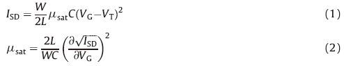
Based on the aligned crystals, we proceeded to fabricate FETs by depositing Au source and drain electrodes through a shadow mask in a top-contact, bottom-gate configuration (Fig. 3d). Since the crystals did not fully cover the channel, the active W/L value was measured to calculate the mobility (Fig. 3e). All the devices were tested in the N2 glovebox, and the saturation regime mobility was calculated. The saturation current (ISD) can be obtained by Eq. (1), and then the saturation mobility (μsat) can be extracted using Eq. (2), where W is channel width, L is channel length, VG is gate voltage, VT is threshold voltage, and C is capacitance per unit area of the gate dielectric.

|
Download:
|
| Fig. 3.FET characteristics of PDPPP crystals. (a) Typical transfer and (b) output characteristics of the devices. (c) Histogram of the hole mobility from 40 devices. (d) A schematic representation of the FET configuration, where S is the source, D is the drain and G is the gate. (e) An OM image showing the method ofW/L measurement. L was measured from the real channel length and W was measured from the contacting area of the crystals that cross the source (S) and drain (D) electrodes. W was calculated by the equation: W=∑(W1 +W2)/2. | |
Here, we take PDPPP as an example. The typical transfer and output characteristics of PDPPP are shown in Fig. 3a and b, exhibiting good gate modulation. Histograms of hole mobility for 40 devices from 3 substrates are displayed in Fig. 3c. An average hole mobility (μh) of 0.079 ± 0.026 cm2 V-1 s-1 (range: 0.036- 0.15 cm2 V-1 s-1, Fig. 3c, black bar) was obtained. After heating at 100 ℃ for 1 h and cooling down naturally, an obvious improvement in average hole mobility has been observed. The average hole mobility reached 0.090 ± 0.042 cm2 V-1 s-1 (range: 0.036-0.19 cm2 V-1 s-1, Fig. 3c, red bar). And on-to-off current ratio (Ion/Ioff) > 105, threshold voltages (VT) between -39 V and -62 V were also obtained. The FET characteristics of FPDPPPF and BuPDPPPBu are demonstrated in Fig. S1 in Supporting information. The FET performances of three molecules are summarized in Table 2. BuPDPPPBu molecular shows the average hole mobility of 0.013 ± 0.010 cm2 V-1 s-1 (range: 0.0017-0.040 cm2 V-1 s-1, Fig. S1g). Different from the other two molecules, FPDPPPF molecule exhibits ambipolar transport, with the average hole mobility of 0.036 ± 0.011 cm2 V-1 s-1 (range: 0.017- 0.063 cm2 V-1 s-1, Fig. S1c) and average electron mobility of 0.0018 ± 0.0016 cm2 V-1 s-1 (range: 0.00015-0.008 cm2 V-1 s-1, Fig. S1f). The emergence of electron transport in this molecule is attributed to the lowered LUMO level due to the strong electronwithdrawing F substituents [30, 31, 32, 33].
|
|
Table 2 Hole and electron transport performance of PDPPP, FPDPPPF and BuPDPPPBu after heating. |

The achieved holemobilities areamong the highest values for the DPP-based small molecules, but they are much lower than the highperformance DPP-based polymers. In order to figure out the reason of the low mobility, we investigated the surface morphology of crystals with the aid of AFM (Fig. 2g-l). The AFM images of three crystals demonstrated their relative rough surface. In the detail images (Fig. 2j-l), the surface of the crystals is roughwithmany steps (RMS (root mean square) roughness ~1.2-4.6 nm). As a supporting evidence for the rough surface, the OM images of these crystals exhibit slightly different contrast along the crystals (Fig. 2a-f). The surface roughness is much larger than that of the typical spin coated polymer films (RMS roughness ~1 nm [34]). The rough crystal surfaces lead to poor contact interfaces between the crystals and the dielectrics and, thus, non-smooth charge transport channels. The rough crystal surfaces might be due to the long-branched alkyl side chains, which are bulky enough to hinder efficient intermolecular interactions and molecular packing, affecting adversely the charge transport. In addition, the existence of macro-steps in the crystal surfaces indicates the fast growth rate and further control on the growth kinetics might improve the crystal morphology.
4. ConclusionIn summary, we have grown aligned crystals of three DPP-based small molecules from para-xylene. Although PDPPP molecular showed high hole mobility up to 0.19 cm2 V-1 s-1, which is of the same order of magnitude as reported highest hole mobility for DPP-based small molecules, their charge mobility is still low compared with that in DPP-based polymer. The relative low mobility is associated with the rough crystal surfaces that form poor contact with the dielectrics. This work indicates a possible reason for the low charge mobility of DPP-based small molecules.
AcknowledgmentsThis work was supported by the 973 Program (No. 2014CB643503), National Natural Science Foundation of China (Nos. 51373150, 51461165301), Zhejiang Province Natural Science Foundation (No. LZ13E030002) and Fundamental Research Funds for the Central Universities.
Appendix A. Supplementary dataSupplementary data associated with this article can be found, in the online version, at http://dx.doi.org/10.1016/j.cclet.2016.01.054.
| [1] | M.J. Kang, K.J. Baeg, D. Khim, Y.Y. Noh, D.Y. Kim, Printed, flexible, organic nanofloating-gate memory:effects of metal nanoparticles and blocking dielectrics on memory characteristics, Adv. Funct. Mater. 23(2013) 3503-3512. |
| [2] | J.K. Wu, C.C. Fan, G.B. Xue, et al., Interfacing solution-grown C60 and (3-Pyrrolinium)(CdCl3) single crystals for high-mobility transistor-based memory devices, Adv. Mater. 27(2015) 4476-4480. |
| [3] | G.H. Gelinck, H.E.A. Huitema, E. van Veenendaal, et al., Flexible active-matrix displays and shift registers based on solution-processed organic transistors, Nat. Mater. 3(2004) 106-110. |
| [4] | T. Sekitani, T. Yokota, U. Zschieschang, et al., Organic nonvolatile memory transistors for flexible sensor arrays, Science 326(2009) 1516-1519. |
| [5] | Y.B. Yuan, G. Giri, A.L. Ayzner, et al., Ultra-high mobility transparent organic thin film transistors grown by an off-centre spin-coating method, Nat. Commun. 5(2014) 3005. |
| [6] | V. Podzorov, E. Menard, A. Borissov, et al., Intrinsic charge transport on the surface of organic semiconductors, Phys. Rev. Lett. 93(2004) 086602. |
| [7] | Y. Diao, B.C.K. Tee, G. Giri, et al., Solution coating of large-area organic semiconductor thin films with aligned single-crystalline domains, Nat. Mater. 12(2013) 665-671. |
| [8] | C. Luo, A.K.K. Kyaw, L.A. Perez, et al., General strategy for self-assembly of highly oriented nanocrystalline semiconducting polymers with high mobility, Nano Lett. 14(2014) 2764-2771. |
| [9] | J. Takeya, M. Yamagishi, Y. Tominari, et al., Very high-mobility organic singlecrystal transistors with in-crystal conduction channels, Appl. Phys. Lett. 90(2007) 102120. |
| [10] | I. Kang, H.J. Yun, D.S. Chung, S.K. Kwon, Y.H. Kim, Record high hole mobility in polymer semiconductors via side-chain engineering, J. Am. Chem. Soc. 135(2013) 14896-14899. |
| [11] | H.Y. Li, B.C.K. Tee, J.J. Cha, et al., High-mobility field-effect transistors from largearea solution-grown aligned C60 single crystals, J. Am. Chem. Soc. 134(2012) 2760-2765. |
| [12] | G.B. Xue, C.C. Fan, J.K. Wu, et al., Ambipolar charge transport of TIPS-pentacene single-crystals grown from non-polar solvents, Mater. Horiz. 2(2015) 344-349. |
| [13] | G.B. Xue, J.K. Wu, C.C. Fan, et al., Boosting the electron mobility of solution-grown organic single crystals via reducing the amount of polar solvent residues, Mater. Horiz. (2016), http://dx.doi.org/10.1039/C5MH00190K. |
| [14] | J. Liu, H.T. Zhang, H.L. Dong, et al., High mobility emissive organic semiconductor, Nat. Commun. 6(2015) 10032. |
| [15] | J.H. Dou, Y.Q. Zheng, Z.F. Yao, et al., A cofacially stacked electron-deficient small molecule with a high electron mobility of over 10 cm2 V-1 s-1 in air, Adv. Mater. 27(2015) 8051-8055. |
| [16] | F.J. Zhang, Y.B. Hu, T. Schuettfort, et al., Critical role of alkyl chain branching of organic semiconductors in enabling solution-processed N-channel organic thinfilm transistors with mobility of up to 3.50 cm2 V-1 s-1, J. Am. Chem. Soc. 135(2013) 2338-2349. |
| [17] | Z.R. Yi, S. Wang, Y.Q. Liu, Design of high-mobility diketopyrrolopyrrole-based pconjugated copolymers for organic thin-film transistors, Adv. Mater. 27(2015) 3589-3606. |
| [18] | M.J. Cho, J. Shin, S.H. Yoon, et al., A high-mobility terselenophene and diketopyrrolopyrrole containing copolymer in solution-processed thin film transistors, Chem. Commun. 49(2013) 7132-7134. |
| [19] | Y.L. Qiao, Y.L. Guo, C.M. Yu, et al., Diketopyrrolopyrrole-containing quinoidal small molecules for high-performance, air-stable, and solution-processable nchannel organic field-effect transistors, J. Am. Chem. Soc. 134(2012) 4084-4087. |
| [20] | H.J. Chen, Y.L. Guo, G. Yu, et al., Highly π-extended copolymers with diketopyrrolopyrrole moieties for high-performance field-effect transistors, Adv. Mater. 24(2012) 4618-4622. |
| [21] | J. Lee, A.R. Han, J. Kim, et al., Solution-processable ambipolar diketopyrrolopyrrole-selenophene polymer with unprecedentedly high hole and electron mobilities, J. Am. Chem. Soc. 134(2012) 20713-20721. |
| [22] | J. Lee, A.R. Han, H. Yu, et al., Boosting the ambipolar performance of solutionprocessable polymer semiconductors via hybrid side-chain engineering, J. Am. Chem. Soc. 135(2013) 9540-9547. |
| [23] | J. Li, Y. Zhao, H.S. Tan, et al., A stable solution-processed polymer semiconductor with record high-mobility for printed transistors, Sci. Rep. 2(2012) 754. |
| [24] | J.Y. Back, H. Yu, I. Song, et al., Investigation of structure-property relationships in diketopyrrolopyrrole-based polymer semiconductors via side-chain engineering, Chem. Mater. 27(2015) 1732-1739. |
| [25] | B. Sun, W. Hong, Z.Q. Yan, H. Aziz, Y.N. Li, Record high electron mobility of 6.3 cm2 V-1 s-1 achieved for polymer semiconductors using a new building block, Adv. Mater. 26(2014) 2636-2642. |
| [26] | H.J. Yun, S.J. Kang, Y. Xu, et al., Dramatic inversion of charge polarity in diketopyrrolopyrrole-based organic field-effect transistors via a simple nitrile group substitution, Adv. Mater. 26(2014) 7300-7307. |
| [27] | S.L. Suraru, U. Zschieschang, H. Klauk, F. Würthner, Diketopyrrolopyrrole as a pchannel organic semiconductor for high performance OTFTs, Chem. Commun. 47(2011) 1767-1769. |
| [28] | W.S. Yoon, S.K. Park, I. Cho, et al., High-mobility n-type organic transistors based on a crystallized diketopyrrolopyrrole derivative, Adv. Funct. Mater. 23(2013) 3519-3524. |
| [29] | H.Q. Shi, Z.W. Gu, X. Gu, et al., Effect of end-groups on the photovoltaic property of diphenyl substituted diketopyrrolopyrrole derivatives, Synth. Met. 188(2014) 66-71. |
| [30] | J.C. Huang, H.Y. Li, X. Mo, et al., Crystal growth and characterization of fluorinated perylene diimides, Chem. Res. Chin. Univ. 30(2014) 63-67. |
| [31] | J.G. Mei, Y. Diao, A.L. Appleton, L. Fang, Z.N. Bao, Integrated materials design of organic semiconductors for field-effect transistors, J. Am. Chem. Soc. 135(2013) 6724-6746. |
| [32] | K. Zhou, H.L. Dong, H.L. Zhang, W.P. Hu, High performance n-type and ambipolar small organic semiconductors for organic thin film transistors, Phys. Chem. Chem. Phys. 16(2014) 22448-22457. |
| [33] | J. Huang, D. Wu, H.J. Ge, S.H. Liu, J. Yin, Fluorinated 1, 8-naphthalimides:synthesis, solid structure and properties, Chin. Chem. Lett. 25(2014) 1399-1402. |
| [34] | H.Y. Li, J.G. Mei, A.L. Ayznera, et al., A simple droplet pinning method for polymer film deposition for measuring charge transport in a thin film transistor, Org. Electron. 13(2012) 2450-2460. |