 2015, Vol.26


 , Qi-Huang Gonga,c
b International Center for Quantum Materials, School of Physics, Peking University, Beijing 100871, China;
c Collaborative Innovation Center of Quantum Matter, Beijing 100871, China
Owing to the excellent photoelectronic properties,such as high charge carrier mobility,luminescence and light harvesting characteristics,hybrid organic-inorganic halide perovskites have attracted increasing attention in past years [1, 2, 3, 4]. The efficiency of perovskite solar cells increased from 3.8% in 2009 to 20.1% in 2015 [4, 5, 6, 7, 8, 9, 10, 11, 12, 13, 14, 15]. Optimizing the processing methods for perovskite films is one of the keys to improve the device performance. Normally, methods for preparing perovskite films may simply be divided into co-evaporation methods and solution-processed methods. The coevaporation method is easy to control and guarantees perovskite films with full coverage and uniformity. However,the requirement of high vacuum increases the cost and limits its use in mass production [8, 16, 17]. Solution methods offer more alternatives for fabricating perovskite solar cells through high-throughput and cost-effective approaches [18]. In the traditional solutionprocessed methods,such as the spin-coating process,a large proportion of perovskite precursor solutions containing Pb are not turned into the final perovskite film during the coating process, which causes a huge waste of precursor materials and potential pollution to the environment.
In this work,a fast-growing procedure (FGP) is demonstrated to fabricate the perovskite film by dropping the precursor solutions onto the substrates at a temperature of ~240 °C. Due to the high processing temperature,the solvent in the precursor solution evaporates quickly in about 2 s,resulting in the fast formation of perovskite film without further annealing with all the precursor materials turn into the final perovskite film without any lost. Millimeter-scale perovskite grain clusters could be obtained in the film fabricated through the FGP [19, 20]. Based on such perovskite films,planar heterojunction perovskite solar cells were fabricated, giving a PCE above 8%.
2. Experimental 2.1. Material and substrate preparationLead iodide (PbI2) and [6, 6]-phenyl-C61-butyric acid methyl ester (PC61BM)werepurchased fromSigmaAldrich.2,20,7,70-tetrakis[N,Ndi(4-methoxyphenyl)amino]-9,90-spirobifluorene (Spiro-OMeTAD) was purchased from SunaTech,and poly(3,4-ethylenedioxythiophene):poly(styrene sulfonate) (PEDOT:PSS) was purchased from Guangzhou Aibot Synthetic Material. All liquid reagents,such as N,N-dimethylformamide (DMF) and chlorobenzene (CB),were purchased from commercial sources (Acros) and used as received.
The perovskite precursor solution was obtained via mixing an equimolar mixture of PbI2 and methylamine hydrochloride (MACl) in DMF at the concentration of ~10 mg/mL.
The fluorine doped tin oxide (FTO) glass (15 V/sq) was etched with zinc powder and HCl (2 mol/L) to obtain the required electrode pattern.
2.2. TiO x flat film precursor solution [21]The TiO x flat film precursor solution consists of 0.23 mol/L titanium isopropoxide (Sigma-Aldrich,99.999%) and 0.013 mol/L HCl solution in isopropanol (99.9% Fisher Chemicals). To prepare this solution,titanium isopropoxide (369 mL) was diluted in isopropanol (2.53 mL) at 0.46 mol/L. Separately,a 2 mol/L HCl solution (35 mL) was diluted with isopropanol (2.53 mL) to achieve a 0.026 mol/L concentration. Finally,the acid-containing solution was added dropwise to the titanium precursor solution under heavy stirring. The solution was filtered with a PTFE filter with 0.22 mm pore size before use.
2.3. Regular structure device fabricationThe regular structure devices were fabricated on pre-patterned FTO glass substrates which were sequentially cleaned with diluted detergent,deionized water,acetone,and isopropanol (IPA). Then, the TiO2 layer was deposited by spin coating the TiOx precursor solution at 3000 rpm for 60 s followed by heating at 500 °C for 30 min. Then the TiO2 coated substrates were kept at 240 °C. At the same time,the perovskite precursor solution was kept at 150 °C. About 40 mL of the perovskite solution was dropped onto the hot TiO2 film and spread quickly. As soon as the films turned dark,they should be transferred away from the hotplate to cool down,giving the finished perovskite films. The p-type Spiro-OMeTAD (80 mg of Spiro-OMeTAD,17.5 mL of lithium bis(trifluoromethanesulfonyl) imide (Li-TFSI) solution (520 mg of Li-TFSI in 1 mL of acetonitrile) and 28.5 mL of 4-tert-butylpyridine all dissolved in 1 mL of CB) was then coated on perovskite active layer as the hole transporting layer. Finally,80 nm of gold was evaporated onto the device through a shadow mask (0.09 cm2).
2.4. Inverted structure device fabricationThe inverted structure devices were fabricated on prepatterned indium tin oxide (ITO) glass substrates which were sequentially cleaned with diluted detergent,deionized water, acetone,and IPA. The PEDOT:PSS was spin coated onto the ITO substrates at 3000 rpm for 30 s. The samples were then heated at 120 °C for 15 min in ambient atmosphere before being transferred to a N2 glove box. Then the PEDOT:PSS coated substrates were kept at 240 °C. At the same time,the perovskite precursor solution was kept at 150 °C. About 40 mL of the perovskite solution was dropped onto the hot PEDOT:PSS films and spread quickly. As soon as the films turned dark,they should be transferred away from the hot plate to cool down,giving the finished perovskite films. A 35 mL of PC61BM solution (40 mg/mL in CB) was then spin coated onto the perovskite layer. Finally,100 nm of aluminum was deposited as the back contact (0.09 cm2) through thermal evaporation.
2.5. Device characterizationThe devices were illuminated under 100 Mw/cm2 by a 150 W Class AAA solar simulator (XES-40S1,SAN-EI) with an AM 1.5G filter. Light intensity of 100 mW/cm2 was determined by a standard monocrystal silicon photodiode calibrated by the Newport TAC-PV lab. The current-voltage curves were measured using a Keithley 2400 source-measure unit. The regular structure-based devices were measured under ambient conditions at room temperature without encapsulation (temperature ~20 °C,humidity ~30%). The measurements of the inverted structure devices were performed in a N2 glove box at room temperature without encapsulation. Scanning electron microscopy (SEM) images were collected by an FEI Nova NanoSEM 430 field-emission SEM. The film thickness was measured by stylus profilometry (Bruker Dektak XT).
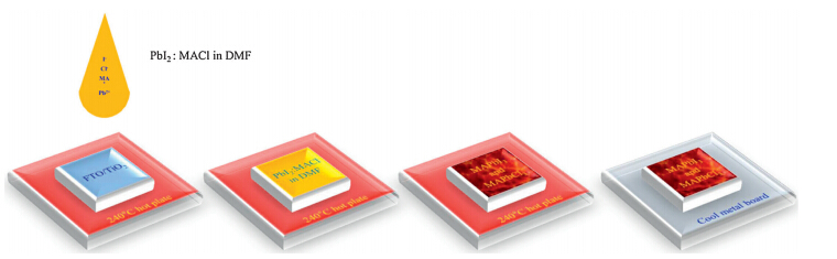
3. Results and discussionFig.1 shows the details of the FGP for perovskite films. The perovskite precusor solution used here was an equimolar mixture of PbI2 and MACl in DMF at the concentration of ~10 mg/mL. Firstly,a dense TiO2 layer coated FTO substrate or a PEDOT:PSS coated ITO substrate was placed on a hotplate at 240 °C in air. At the same time,the perovskite precursor solution was also maintained at about 150 °C. Then,about 40 mL of the hot perovskite solution was dropped onto the hot substrate. The solution spread quickly on the substrate and formed a deep dark film within 2 s. As soon as the sample turned dark,it would be transferred away from the hotplate to cool to room temperature, giving the finished perovskite film. Due to the high temperature of the substrate,the finished perovskite film did not require further thermal annealing process,which is commonly used in the regular solution-process for perovskite films. Thus,the FGP could avoid the thermal annealing process and ensure the fast formation of perovskite films within a couple of seconds.

|
Download:
|
| Fig. 1. Schematic of fast-growing procedure for perovskite films. | |
The scan electron microscopy (SEM) image was taken to observe the surface morphology of the perovskite film based on the FGP method. As shown in Fig.2a,the pinhole-free perovskite film was obtained,which covered the entire substrate with less cracks or visible large grain boundaries. The grain clusters with a size of about 1 mm could be formed,which consisted of close-packed perovskite crystal grains. The size of grain clusters was even larger than the thickness of the film,which was about 800 nm. As reported in previous literature [22, 23],a larger grain size could ensure the effective charge collection by electrodes,which was favorable for high-performance devices. Fig.2b showed the optical microscopy image for the perovskite film obtained from the FGP method. The optical microscopy image was taken using the transmission mode,which revealed that the substrate was fully covered by the perovskite film without any visible pin-holes. This is in consistent with the conclusion drawn from the SEM image.

|
Download:
|
| Fig. 2. (a) The SEM image and (b) optical micrograph of the perovskite film. | |
Generally,it is believed that methylamine lead halide perovskites are not stable at high temperature over 150 °C [12, 24, 25]. The perovskite layer may be decomposed to PbI2 due to the high temperature. In the current FGP methods,the film formation was processed at a high temperature of ~240 °C. Thus,to investigate the potential decomposition of the perovskite film fabricated by the FGP method,X-ray diffraction (XRD) analysis was conducted to study the crystalline phases present in the film. Fig.3 shows the XRD pattern of the perovskite film based on FGP. The XRD pattern of pure PbI2 is also provided in Fig.3 for comparison. Pure PbI2 exhibits the characteristic peak at 12.688. However,it is obvious that no peak at 12.688 is found in the XRD spectrum of the perovskite film fabricated by the FGP,indicating that the perovskite film had not decomposed during the FGP. This could be ascribed to the fast process of only ~2 s,which was too short for the perovskite film to undergo decomposition,although the substrate temperature was about 240 °C. It was also determined that the film still could suffer from decomposition if the film was kept on the 240 °C hot plate for a longer time. The film would turn from dark brown to yellow if the heating lasted for another 3 s. Thus,avoiding increased time and substrate temperature are critical for the fast formation of the perovskite film in the FGP method.

|
Download:
|
| Fig. 3. XRD spectra of the PbI2 film and the perovskite film. | |
In order to evaluate the quality of the film,perovskite solar cells with both regular and inverted structures were constructed based on perovskite films prepared by the FGP method. Fig.4a and b shows the device architectures. For devices with the regular structure,dense TiO2 was chosen as the electron transport layer (ETL) and Spiro-OMeTAD was chosen as the hole transport layer (HTL). While for devices with the inverted structure,PEDOT:PSS and PC61BM were chosen as HTL and ETL,respectively. Fig.4c and d shows the preliminary current density-voltage (J-V) characterization for the regular and inverted devices,respectively. The device with the regular structure achieved a short-circuit current density (Jsc) of 17.9 mA/cm2,an open circuit voltage (Voc) of 0.95 V,a fill factor (FF) of 0.51 and a PCE of 8.7%,while the device with the inverted structure delivered a Jsc of 10.6 mA/cm2,an Voc of 0.93 V,a FF of 0.53 and a PCE of 5.2%. The relatively lower Jsc in the inverted structure device might be attributed to the destroyed PEDOT:PSS film at 240 °C,which could be improved if other HTL candidates can be used to replace the less stable PEDOT:PSS layer.
4. ConclusionIn conclusion,we have demonstrated a simple fast-growing procedure (FGP) for making perovskite films. In this approach,the solvent in the precursor solution is removed in only 2 s,resulting in the fast formation of perovskite film without further annealing. All the precursor materials could be turned into the final perovskite film without any lost. Millimeter-scale perovskite grain clusters are obtained in the film fabricated by the FGP. Based on such perovskite films,planar heterojunction perovskite solar cells were fabricated,giving a PCE above 8%. Our future work will focus on optimizing the film morphology and composition,thus perovskite solar cells with higher efficiency can be expected.
AcknowledgmentsThis work was financially supported by the National Natural Science Foundation of China (Nos. 61377025,91433203, 11121091) and the 973 Program of China (No. 2015CB932203). The authors thank Prof. Xinqiang Wang for the calibration of solar simulator.
| [1] | J. Shi, X. Xu, D. Li, et al., Interfaces in perovskite solar cells, Small 11 (2015) 2472-2486. |
| [2] | L. Zheng, D. Zhang, Y. Ma, et al., Morphology control of the perovskite films for efficient solar cells, Dalton Trans. 44 (2015) 10582-10593. |
| [3] | J.P. Wang, N.N. Wang, Y.Z. Jin, et al., Interfacial control toward efficient and lowvoltage perovskite light-emitting diodes, Adv. Mater. 27 (2015) 2311-2316. |
| [4] | A. Kojima, K. Teshima, Y. Shirai, et al., Organometal halide perovskites as visiblelight sensitizers for photovoltaic cells, J. Am. Chem. Soc. 131 (2009) 6050-6051. |
| [5] | J.H. Im, C.R. Lee, J.W. Lee, et al., 6.5% efficient perovskite quantum-dot-sensitized solar cell, Nanoscale 3 (2011) 4088-4093. |
| [6] | H.S. Kim, C.R. Lee, J.H. Im, et al., Lead iodide perovskite sensitized all-solid-state submicron thin film mesoscopic solar cell with efficiency exceeding 9%, Sci. Rep. 2 (2012) 591. |
| [7] | S.D. Stranks, G.E. Eperon, G. Grancini, et al., Electron-hole diffusion lengths exceeding 1 micrometer in an organometal trihalide perovskite absorber, Science 342 (2013) 341-344. |
| [8] | M. Liu, M.B. Johnston, H.J. Snaith, Efficient planar heterojunction perovskite solar cells by vapour deposition, Nature 501 (2013) 395-398. |
| [9] | J. Burschka, N. Pellet, S.-J. Moon, et al., Sequential deposition as a route to highperformance perovskite-sensitized solar cells, Nature 499 (2013) 316-319. |
| [10] | A. Mei, X. Li, L. Liu, et al., A hole-conductor-free, fully printable mesoscopic perovskite solar cell with high stability, Science 345 (2014) 295-298. |
| [11] | G. Xing, N. Mathews, S. Sun, et al., Long-range balanced electron- and hole-transport lengths in organic-inorganic CH3NH3PbI3, Science 342 (2013) 344-347. |
| [12] | Q. Hu, J. Wu, C. Jiang, et al., Engineering of electron-selective contact for perovskite solar cells with efficiency exceeding 15%, ACS Nano 8 (2014) 10161-10167. |
| [13] | H. Zhou, Q. Chen, G. Li, et al., Interface engineering of highly efficient perovskite solar cells, Science 345 (2014) 542-546. |
| [14] | N.J. Jeon, J.H. Noh, W.S. Yang, et al., Compositional engineering of perovskite materials for high-performance solar cells, Nature 517 (2015) 476-480. |
| [15] | W.S. Yang, J.H. Noh, N.J. Jeon, et al., High-performance photovoltaic perovskite layers fabricated through intramolecular exchange, Science 348 (2015) 1234-1237. |
| [16] | Q. Chen, H. Zhou, Z. Hong, et al., Planar heterojunction perovskite solar cells via vapor-assisted solution process, J. Am. Chem. Soc. 136 (2014) 622-625. |
| [17] | O. Malinkiewicz, A. Yella, Y.H. Lee, et al., Perovskite solar cells employing organic charge-transport layers, Nat. Photonics 8 (2014) 128-132. |
| [18] | T. Salim, S. Sun, Y. Abe, et al., Perovskite-based solar cells: Impact of morphology and device architecture on device performance, J. Mater. Chem. A 3 (2015) 8943-8969. |
| [19] | M. Xiao, F. Huang, W. Huang, et al., A fast deposition-crystallization procedure for highly efficient lead iodide perovskite thin-film solar cells, Angew. Chem. Int. Ed. 126 (2014) 10056-10061. |
| [20] | W. Nie, H. Tsai, R. Asadpour, et al., High-efficiency solution-processed perovskite solar cells with millimeter-scale grains, Science 347 (2015) 522-525. |
| [21] | P. Docampo, J.M. Ball, M. Darwich, et al., Efficient organometal trihalide perovskite planar-heterojunction solar cells on flexible polymer substrates, Nat. Commun. 4 (2013) 2761. |
| [22] | Z. Xiao, Q. Dong, C. Bi, et al., Solvent annealing of perovskite-induced crystal growth for photovoltaic-device efficiency enhancement, Adv. Mater. 26 (2014) 6503-6509. |
| [23] | J.H. Im, I.H. Jang, N. Pellet, et al., Growth of CH3NH3PbI3 cuboids with controlled size for high-efficiency perovskite solar cells, Nat. Nanotechnol. 9 (2014) 927-932. |
| [24] | Q. Hu, Y. Liu, Y. Li, et al., Efficient and low-temperature processed perovskite solar cells based on a cross-linkable hybrid interlayer, J. Mater. Chem. A (2015) 18483-18491. |
| [25] | Q. Chen, H. Zhou, T.-B. Song, et al., Controllable self-induced passivation of hybrid lead iodide perovskites toward high performance solar cells, Nano Lett. 14 (2014) 4158-4163. |