


b Program in Applied Physics, University of Michigan, Ann Arbor, MI 48109-1040, USA
Organic solar cells have the potential for large-scale,inexpensive solar cell production [1],conversely,the highest performance photovoltaics are constructed from entirely crystalline inorganic semiconductors. Recent research efforts have focused on developing hybrid organic-inorganic solar cell architectures to combine the best aspects of each [2, 3]. Several types of hybrid organic-inorganic solar cells have shown notable power conversion efficiencies,such as nanostructured ZnO [4, 5],GaAs [6, 7],TiO2/perovskite [8],and Si [9, 10, 11]. However,platforms where the inorganic semiconductor is the medium for photogeneration of charge carriers and the organic material is an optically transparent,carrier-selective contact are particularly attractive. These constructs can hypothetically utilize the broadband absorption and good charge transport properties of inorganic semiconductorswhile avoiding the Fermi-level pinning in traditional metal-semiconductor junctions since the organic material rarely has any metallurgical reactivity with the semiconductor.
Highly conductive,transparent polymer blend poly(3,4-ethylenedioxythiophene): poly(4-styrene sulfonate) (PEDOT:PSS),is soluble in water,non-toxic,and can be deposited by inexpensive, high-throughput methods such as roll-to-roll and ink jet printing [12, 13, 14, 15]. In heterojunctions,PEDOT:PSS can act as a hole-selective layer which helps to suppress dark currents [16, 17, 18, 19]. We have previously demonstrated that PEDOT:PSS significantly augments, relative to metals with similar work functions,the attainable photovoltage values in heterojunctions involving n-Si [20].
No work has been done to develop hybrid organic-inorganic solar cells using PEDOT:PSS and gallium phosphide (GaP). The midsized band gap (2.26 eV) and the capacity for large charge carrier mobilities in GaP afford substantially larger photovoltages than Si under the same illumination intensity. Photocells that generate large electromotive forces are useful in combination with electrolytic reactors in the context of electrochemical energy conversion and storage [21, 22, 23, 24, 25, 26, 27]. A disadvantage with GaP relative to Si is that the charge-carrier lifetimes and apparent chargecarrier diffusion lengths are extremely short,increasing the probability of deleterious recombination of photogenerated carriers and thereby limiting photocurrent from the absorption of visible light. We and others have shown previously that nanostructuring GaP so as to impart a high aspect ratio can ameliorate the short lifetimes and diffusion lengths and thus attain the maximum possible photocurrent values [28, 29, 30].
Herein,we report the fabrication of n-type macroporous GaP and PEDOT:PSS hybrid devices and their response characteristics under white light illumination. Values of the open-circuit voltage (Voc),short-circuit photocurrent density (Jsc),fill factor (FF),and total energy conversion efficiency were evaluated from steadystate current-voltage measurements. Light absorption properties were measured so as to assess both external and internal quantum yields of these constructs. The effects of doping density and surface modification with gold nanoparticles on device performance were also evaluated and reported here. 2. Experimental 2.1. Device fabrication
Polished n-type GaP(1 0 0) wafers were purchased from El-Cat with dopant densities of 5×10¹⁷ and 1×1018 cm-3. Ohmic contact with In films was achieved as previously reported [28]. The procedure used for the anodic etching of planar n-type GaP to macroporous structure was the same as described previously [28]. The duration of etching was sufficiently long (t > 120 min) to ensure that pore depths exceeded 45 μm. An aqueous solution containing 25% (v/v) PEDOT:PSS (Clevios P),5% DMSO (BDH, 99.9%),and 1% Triton X-100 (USB Corporation) was prepared for spin-coating. A 0.1 mL drop of PEDOT:PSS solution was dropped on a GaP sample masked with an exposed area of ~0.5 cm2 and allowed to air dry. During drying,the sample was spun at a rate of 300 rpm for 10 min. To contact the dried PEDOT:PSS layer,a drop of silver print (GC Electronics) was placed atop outside of the masked area to minimize light blockage. A representative schematic of the hybrid solar cell is shown in Fig. 1a.

|
Download:
|
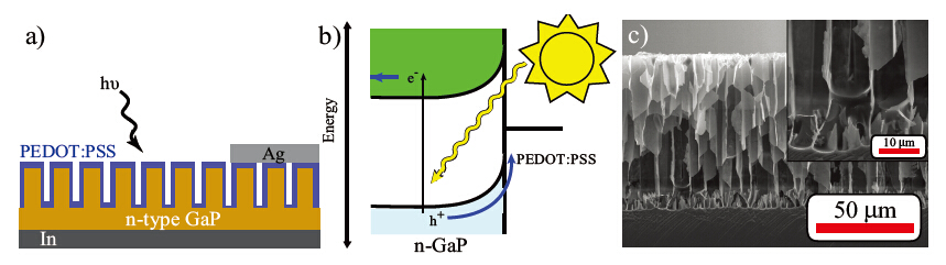
| Fig. 1. Schematics of (a) the GaP/PEDOT:PSS hybrid solar cell and of (b) the corresponding band structure diagram and charge transfer process under illumination. In (c),a representative scanning electron micrograph showed macroporous GaP uniformly coated with <100 nm layer of PEDOT:PSS. | |
After anodic etching,the macroporous sample was soaked in 10% cysteamine (Sigma-Aldrich,95%) in ethanol solution for 2 h, rendering a macroporous surface covered with thiol groups. The treated sample was rinsed with distilled water (>18 MΩ cm, Barnstead Nanopure III purifier),dried with flowing nitrogen gas, and then immersed in an aqueous solution with 12 nm gold nanoparticles. Gold nanoparticle suspensions were prepared by a slightly modified Turkevich method [31],through the reduction of aqueous HAuCl4 (Strem Chemicals) by N3C6H5O7 (J.T. Baker) under reflux. After 20 min of immersion,the sample was rinsed with distilled water and dried with a stream of nitrogen gas. This procedure affected a monolayer of gold nanoparticles linked by thiol group formed on the surface of the macroporous structures. To improve gold nanoparticle coverage,the sample was subsequently soaked in an aqueous solution containing 0.1 mol L-1 KCl (Mallinckrodt) and 0.3 mmol L-1 HAuCl4 until the yellow porous structure darkened. The sample was then coated with PEDOT:PSS as described above. 2.3. Characterization
Scanning electron microscopic analysis of the macroporous structure was conducted with a Philips XL-ESEM instrument operated at 15 kV with a secondary electron detector. Pore depths and polymer infiltration were assessed directly from electron micrographs. External quantum yield and diffuse reflectance were measured with apparatus as previously noted [28, 29]. Steady-state current-voltage measurements were carried out using a CHI 420 potentiostat under light from an ELH tungsten-halogen lamp. Illumination intensities were measured using a digital Optical Power Meter PM100 (Thorlabs). 3. Results and discussion
Fig. 1b shows the general energy-band diagram expected for the n-GaP/PEDOT:PSS heterojunction under illumination. The expectation is that the photo effect is governed by the properties of the n- GaP material. A representative scanning electron micrograph is shown in Fig. 1c,demonstrating the even coating of the PEDOT:PSS polymer (<100 nm thickness) throughout the high-aspect ratio GaP pores. For PEDOT:PSS formulations different than those described above,the PEDOT:PSS layer did not uniformly coat the sidewalls.
Fig. 2a shows current-voltage characteristics under 100mWcm-2 white light illumination for n-type planar GaP (black) and macroporous GaP coated with a thin layer (<100 nm) PEDOT:PSS (blue). The pertinent response metrics are shown in Table 1. The heterojunctions with macroporous GaP consistently gave enhanced photoresponse characteristics than those heterojunctions with planar GaP. Specifically,macroporous n-GaP films attained a 15-fold increase in total energy conversion efficiency relative to the planar GaP films. At these conditions,macroporous n-GaP/PEDOT:PSS heterojunctions exhibited Jsc = 2.34 mA cm-2 and Voc = 0.95 V. These solar cell characteristics were comparable with the best published reports for p-n homojunction GaP photovoltaics (Table 1) [32, 33].

|
Download:
|
| Fig. 2. Planar and macroporous GaP coated with PEDOT:PSS were compared by (a) current density-voltage measurements under illumination,(b) external quantum yield,(c) diffuse reflectance,and (d) internal quantum yield. The doping density of GaP was 1×1018 cm-3. | |
| Table 1 Biological activities of pure metabolite6against microbial test organisms in agar diffusion assay.aMeasured hybrid device parameters under 100mWcm-2 white light illumination. |

The improved responses for the macroporous heterojunctions were due to a broadband increase in the charge-collection efficiency of photogenerated charges (Fig. 2b). To determine if the enhancement was purely due to lower specular reflection losses with the macroporous films,diffuse reflectance spectra were obtained. Fig. 2c shows the reflected light from planar and macroporous GaP electrodes coated with an equivalent PEDOT:PSS layer. Macroporous GaP exhibited lower diffuse reflectance only at wavelengths >500 nm. The data in Fig. 2c were used to correct the data in Fig. 2b to identify the wavelength-dependent profile of the internal quantum yield for both planar and macroporous films. These results are shown in Fig. 2d. A comparison of the two profiles showed that although the quantum yield for charge collection was uniformly larger at every wavelength for the nanostructured GaP electrodes,the enhancement was most pronounced at values close to the bandgap energy. These data illustrate that the premise of nanostructuring GaP to eliminate the loss of carriers photogenerated by deeply penetrating light (i.e. light with near bandgap energies) is operative in these solid-state GaP/PEDOT:PSS heterojunctions.
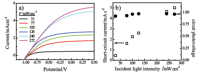
Fig. 3a illustrates the photoresponse characteristics of a macroporous n-GaP/PEDOT:PSS heterojunction at several different illumination intensities. As expected,the photocurrent values at short circuit were strongly sensitive to the illumination conditions. Fig. 3c summarizes the specific dependencies of both the Jsc and Voc with the incident light intensity. The values of Jsc increased linearly with light intensity at a slope of 0.018 mAmW-1. At increasingly higher light intensities,the fill factor deteriorates,suggestive of a rate of 65 mV per decade increase in light intensity.

|
Download:
|
| Fig. 3. The effect of light intensity on the (a) current density-voltage measurements and (b) short-circuit current (open squares) and open circuit photovoltage (filled circles) of macroporous GaP coated with PEDOT:PSS was shown. | |
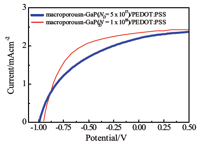
Fig. 4 shows current-voltage data for macroporous n-GaP devices as a function of dopant density within GaP. In Figure, macroporous substrates with dopant concentrations of 5×10¹⁷ and 1×1018 cm-3 are shown. Increased dopant concentration yielded slightly better fill factors and a small increase in Jsc,albeit with a corresponding sacrifice in the value of Voc.

|
Download:
|
| Fig. 4. Current density-voltage measurements under illumination of PEDOT:PSS coated macroporous GaP were shown with different GaP doping densities of 5×10¹⁷ (solid line) and 1×10¹⁸ (dashed line) cm-3,respectively. | |
Surface modification of macroporous GaP with gold nanoparticles was explored as a means to improve the current- voltage response characteristics under illumination. Fig. 5 shows the current-voltage curves obtained in the dark and under illumination for macroporous GaP coated with only PEDOT:PSS and first with Au nanoparticle surface decoration and subsequent PEDOT:PSS coating. The effect of inclusion of Au nanoparticles was to increase Jsc substantially but with a diminution of Voc. The net effect of the changes was to increase the energy conversion efficiency from 1.21% to 1.81%. The same Au nanoparticle surface treatment was also applied to planar n- GaP surfaces. Fig. 6a shows that this surface treatment affected planar n-GaP/PEDOT:PSS heterojunctions in a substantially different manner. Inclusion of Au nanoparticles uniformly deteriorated the Jsc and Voc values. Fig. 6b displays the external quantum yield profile for these two types of planar n-GaP devices. At all wavelengths,inclusion of Au nanoparticles resulted in lower quantum yields.

|
Download:
|
| Fig. 5. Current density-voltage curves for solid-state devices with and without surface modification with Au nanoparticles. The doping density of GaP was 5×1017 cm-3. | |

|
Download:
|
| Fig. 6. The effect of Au nanoparticle surface modification on planar GaP coated with PEDOT:PSS was shown by (a) current density-voltage measurements under illumination and (b) external quantum yield. | |
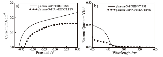
The collective data demonstrate that GaP with high aspect ratios can operate effectively with respect to light collection and charge separation in solid state devices over planar GaP substrates. These results corroborate the increased light conversion properties of macroporous GaP in photoelectrochemical systems [28]. Enhanced photoresponse was observed for macroporous structured GaP over planar GaP in hybrid organic-inorganic solar cell devices.
The main benefit of this solid state device conformation is that using conductive polymer as hole injecting layer is a simple and scalable process,commonly used for roll-to-roll and ink jet processing of organic photovoltaic devices [12, 13]. The key technical achievement of this work was finding a formulation that allowed a thin layer of PEDOT:PSS to penetrate the deep pores (>50 μm) of the macroporous GaP. This breakthrough allows for the full light harvesting and charge separating benefits of the high aspect ratio GaP structure as well as high surface area contact to the hole injecting layer of PEDOT:PSS.
Macroporous GaP/PEDOT:PSS solid state devices showed enhanced photocurrent in Fig. 2. This enhancement was likely due to the absorption and utilization of the longer wavelengths of light (450-550 nm). Quantum yield measurements indicated an increase in this region (Fig. 2b). Another important quality of these devices was that they maintained sufficient photovoltage in this configuration (Voc = 0.95 V),compared to 1.06 V for photoelectrochemical electrodes [28].
Device configuration was not optimized. In Fig. 3b,we expected logarithmic dependence of Voc on light intensity and measured values did not follow this relationship. This could indicate a device that is not fully ideal. GaP has been known to suffer from lacking interfacial charge transfer properties,most commonly due to surface defects that serve as traps for charge recombination [34]. These traps were mitigated through surface reaction of Ga atoms through Grignard chemistry [35, 36, 37] and reaction of P atoms through Williamson ether-type chemistry [38]. Applying these techniques to the macroporous GaP in these solid state devices could improve the ideality of the device parameters.
In addition to applying surface chemistry techniques,other methods could be used to improve device performance. For example,gold nanoparticles increased the conductivity [39] of PEDOT:PSS and improved total efficiency of ZnO devices [40]. As a result of a gold nanoparticle layer on macroporous GaP,Fig. 5 shows increased photocurrent. Voc and Jsc shifted to 0.88 V and 3.53 mA cm-2,respectively. Notably,the overall efficiency increased to 1.81%. No corresponding amplification of efficiency was observed on planar GaP electrodes. Effects on the optical properties may also be observed [41],but were not tested in this work.
Although the device performance was not optimized,the photoresponse was still sensitive to bulk properties,such as doping density (Fig. 4). The non-ideal influence of surface defects did not preclude either high voltages or large photocurrents. 4. Conclusion
These data show that hybrid solar cells of macroporous GaP with PEDOT:PSS have efficiency of 1.21%. The Jsc and Voc are 2.34 mA cm-2 and 0.95 V,respectively. The macroporous structure of GaP can both enhance the absorption intensity at certain wavelengths and expand the absorption range,which results in higher external quantum yield values. Modifying GaP macroporous surfaces with Au nanoparticles can enhance Jsc to 3.53 mA cm-2 and overall efficiency to 1.81%.
AcknowledgmentsWe thank Dr. J. Gu for his assistance with gold nanoparticle synthesis. This work is supported by the National Science Foundation under Grant # DMR-1054303.
| [1] | B.A. Gregg, Excitonic solar cells, J. Phys. Chem. B 107 (2003) 4688-4698. |
| [2] | W.U. Huynh, J.J. Dittmer, A.P. Alivisatos, Hybrid nanorod-polymer solar cells, Science 295 (2002) 2425-2427. |
| [3] | C. Sanchez, B. Julían, P. Belleville, M. Popall, Applications of hybrid organic- inorganic nanocomposites, J. Mater. Chem. 15 (2005) 3559-3592. |
| [4] | W.J.E. Beek, M.M. Wienk, M. Kemerink, X.N. Yang, R.A.J. Janssen, Hybrid zinc oxide conjugated polymer bulk heterojunction solar cells, J. Phys. Chem. B 109 (2005) 9505-9516. |
| [5] | W.J.E. Beek, M.M. Wienk, R.A.J. Janssen, Efficient hybrid solar cells from zinc oxide nanoparticles and a conjugated polymer, Adv. Mater. 16 (2004) 1009-1013. |
| [6] | G. Mariani, R.B. Laghumavarapu, B.T. de Villers, et al., Hybrid conjugated polymer solar cells using patterned GaAs nanopillars, Appl. Phys. Lett. 97 (2010) 013107. |
| [7] | C.K. Yong, K. Noori, Q. Gao, et al., Strong carrier lifetime enhancement in GaAs nanowires coated with semiconducting polymer, Nano Lett. 12 (2012) 6293-6301. |
| [8] | J.H. Heo, S.H. Im, J.H. Noh, et al., Efficient inorganic-organic hybrid heterojunction solar cells containing perovskite compound and polymeric hole conductors, Nat. Photonics 7 (2013) 487-491. |
| [9] | Y. Ding, R. Gresback, Q.M. Liu, et al., Silicon nanocrystal conjugated polymer hybrid solar cells with improved performance, Nano Energy 9 (2014) 25-31. |
| [10] | V. Svrcek, D. Mariotti, T. Yamanari, K. Matsubara, M. Kondo, Integration of surfactant-free silicon nanocrystal in hybrid solar cells, Jpn. J. Appl. Phys. 51 (2012) 10NE25. |
| [11] | S. Kim, J.H. Lee, M.T. Swihart, J.C. Lee, J.Y. Kim, Silicon nanoparticle size-dependent open circuit voltage in an organic-inorganic hybrid solar cell, Curr. Appl. Phys. 14 (2014) 127-131. |
| [12] | R. Søndergaard, M. Hösel, D. Angmo, T.T. Larsen-Olsen, F.C. Krebs, Roll-to-roll fabrication of polymer solar cells, Mater. Today 15 (2012) 36-49. |
| [13] | F.C. Krebs, S.A. Gevorgyan, J. Alstrup, A roll-to-roll process to flexible polymer solar cells: model studies, manufacture and operational stability studies, J. Mater. Chem. 19 (2009) 5442-5451. |
| [14] | J.Y. Kim, J.H. Jung, D.E. Lee, J. Joo, Enhancement of electrical conductivity of poly(3,4-ethylenedioxythiophene)/poly(4-styrenesulfonate) by a change of solvents, Synth. Met. 126 (2002) 311-316. |
| [15] | R. Steim, F.R. Kogler, C.J. Brabec, Interface materials for organic solar cells, J. Mater. Chem. 20 (2010) 2499-2512. |
| [16] | S.A. Carter, M. Angelopoulos, S. Karg, P.J. Brock, J.C. Scott, Polymeric anodes for improved polymer light-emitting diode performance, Appl. Phys. Lett. 70 (1997) 2067-2069. |
| [17] | Y. Cao, G. Yu, C. Zhang, R. Menon, A.J. Heeger, Polymer light-emitting diodes with polyethylene dioxythiophene-polystyrene sulfonate as the transparent anode, Synth. Met. 87 (1997) 171-174. |
| [18] | H. Ishii, K. Sugiyama, E. Ito, K. Seki, Energy level alignment and interfacial electronic structures at organic/metal and organic/organic interfaces, Adv. Mater. 11 (1999) 605-625. |
| [19] | A. Kahn, N. Koch, W.Y. Gao, Electronic structure and electrical properties of interfaces between metals and p-conjugated molecular films, J. Polym. Sci. Pol. Phys. 41 (2003) 2529-2548. |
| [20] | M.J. Price, J.M. Foley, R.A. May, S. Maldonado, Comparison of majority carrier charge-transfer velocities at Si/polymer and Si/metal photovoltaic heterojunctions, Appl. Phys. Lett. 97 (3) (2010) 083503. |
| [21] | J.F. McCann, L.J. Handley, The photoelectrochemical effect at a p-GaP electrode, Nature 283 (1980) 843-845. |
| [22] | M. Halmann, Photoelectrochemical reduction of aqueous carbon dioxide on ptype gallium phosphide in liquid junction solar cells, Nature 275 (1978) 115-116. |
| [23] | P.A. Kohl, A.J. Bard, Semiconductor electrodes. 13. Characterization and behavior of n-type zinc oxide, cadmium sulfide, and gallium phosphide electrodes in acetonitrile solutions, J. Am. Chem. Soc. 99 (1977) 7531-7539. |
| [24] | J.A. Turner, A realizable renewable energy future, Science 285 (1999) 687-689. |
| [25] | M.P. Dare-Edwards, A. Hamnett, J.B. Goodenough, The efficiency of photogeneration of hydrogen at p-type III/V semiconductors, J. Electroanal. Chem. 119 (1981) 109-123. |
| [26] | C.M. Gronet, N.S. Lewis, Design of a 13% efficient n-GaAs1 xPx semiconductor- liquid junction solar cell, Nature 300 (1982) 733-735. |
| [27] | J.P. Petit, P. Chartier, M. Beley, J.P. Deville, Molecular catalysts in photoelectrochemical cells: study of an efficient system for the selective photoelectroreduction of CO2: p-GaP or p-GaAs/Ni(cyclam)2+, aqueous medium, J. Electroanal. Chem. 269 (1989) 267-281. |
| [28] | M.J. Price, S. Maldonado, Macroporous n-GaP in nonaqueous regenerative photoelectrochemical cells, J. Phys. Chem. C 113 (2009) 11988-11994. |
| [29] | W. Wen, A.I. Carim, S.M. Collins, et al., Structural and photoelectrochemical properties of GaP nanowires annealed in NH3, J. Phys. Chem. C 115 (2011) 22652-22661. |
| [30] | J.W. Sun, C. Liu, P.D. Yang, Surfactant-free, large-scale, solution-liquid-solid growth of gallium phosphide nanowires and their use for visible-light-driven hydrogen production from water reduction, J. Am. Chem. Soc. 133 (2011) 19306-19309. |
| [31] | J. Turkevich, P.C. Stevenson, J. Hillier, A study of the nucleation and growth processes in the synthesis of colloidal gold, Discuss. Faraday Soc. 11 (1951) 55-75. |
| [32] | C.R. Allen, J.H. Jeon, J.M. Woodall, Simulation assisted design of a gallium phosphide n-p photovoltaic junction, Sol. Energy Mater. 94 (2010) 865-868. |
| [33] | C.R. Allen, J.M. Woodall, J.H. Jeon, Results of a gallium phosphide photovoltaic junction with an AR coating under concentration of natural sunlight, Sol. Energy Mater. 95 (2011) 2655-2658. |
| [34] | M.A. Butler, D.S. Ginley, P-type GaP as a semiconducting photoelectrode, J. Electrochem. Soc. 127 (1980) 1273-1278. |
| [35] | J. Mukherjee, S. Peczonczyk, S. Maldonado, Wet chemical functionalization of III- V semiconductor surfaces: alkylation of gallium phosphide using a grignard reaction sequence, Langmuir 26 (2010) 10890-10896. |
| [36] | S.L. Peczonczyk, E.S. Brown, S. Maldonado, Secondary functionalization of allylterminated GaP(1 1 1)A surfaces via heck cross-coupling metathesis, hydrosilylation, and electrophilic addition of bromine, Langmuir 30 (2014) 156-164. |
| [37] | E.S. Brown, S.L. Peczonczyk, Z.J. Wang, S. Maldonado, Photoelectrochemical properties of CH3-terminated p-type GaP(1 1 1)A, J. Phys. Chem. C 118 (2014) 11593-11600. |
| [38] | E.S. Brown, S.L. Peczonczyk, S. Maldonado, Wet chemical functionalization of GaP(1 1 1)B through a williamson ether-type reaction, J. Phys. Chem. C 119 (2015) 1338-1345. |
| [39] | A. Yoshida, N. Toshima, Gold nanoparticle and gold nanorod embedded PEDOT: PSS thin films as organic thermoelectric materials, J. Electron. Mater. 43 (2014) 1492-1497. |
| [40] | Z.H. Chen, Y.B. Tang, C.P. Liu, et al., Vertically aligned ZnO nanorod arrays sentisized with gold nanoparticles for schottky barrier photovoltaic cells, J. Phys. Chem. C 113 (2009) 13433-13437. |
| [41] | S. Jayaraman, P.S. Kumar, D. Mangalaraj, et al., Enhanced luminescence and charge separation in polythiophene-grafted, gold nanoparticle-decorated, 1-D ZnO nanorods, RSC Adv. 4 (2014) 11288-11294. |