


b Department of Electrical Engineering and Computer Science, University of Michigan, Ann Arbor, MI 48109, USA
Surface plasmons (SPs) are surface waves whose electromagnetic field is confined to the vicinity of the metal/dielectric interface. When the condition of the resonance is fulfilled,this confinement leads to an enhancement of the electromagnetic field at the interface [1, 2, 3],therefore,this aspect has been utilized in many photonic applications such as optical devices,sensors and optoelectronics [4, 5, 6, 7]. Among them,their effects on organic photovoltaic (OPV) cells have been highlighted [8, 9, 10, 11, 12],because the field enhancement associated with such nanostructures can be potentially effective means to improve the efficiency of OPVs by enhancing the absorption of light even in a very thin organic semiconductor layer. Because exciton generated in organic semiconductor upon light absorption has limited diffusion distance around 10 nm,which is mismatched to the thickness of photoactive layer for efficient light absorption (e.g.hundreds of nanometers scale),there is inevitably trade-off between photogenerated charge collection and light absorption,which should be resolved to achieve high performance OPV devices [13, 14, 15]. Therefore, the approaches utilizing surface plasmon resonance (SPR) that can improve the optical field in OPV without increasing the thickness of photoactive layer,in principle,can be an effective way to address the mismatch problems between the short exciton diffusion length in organic semiconductors and the large thickness required to fully absorb sunlight [16, 17, 18].
Metal nanoparticle system has been extensively studied to apply SPR effect to OPV cells due to the simple preparation steps. Those plasmonic metal nanoparticles can be fabricated by electrodeposition [19],chemical synthesis [20, 21, 22],nanoimprint lithography (NIL) [7],thermal annealing [23],pulse-laser ablation [24] and vapor phase deposition [25]. In general,the effects of those plasmonic nanoparticles on OPV cells are classified by the size of the particles. It has been known that small nanoparticles (<20 nm) can enhance near-field due to the excitation of localized surface plasmon resonance (LSPR),increasing effective absorption, and relatively larger nanoparticles (>40-50 nm) can be subwavelength scattering sites that can trap propagating plane waves of incident light,consequently increasing optical path length in photoactive layer [1, 26, 27, 28]. Those nanoparticles affect the absorption of light in buffer layer or photoactive layer. Besides, periodic metal nanostructures such as nanogratings are also promising candidate as plasmonic light-trapping structure,because geometrical parameters can be easily controlled for the efficient light absorption [1, 7, 11, 12, 29, 30].
In this article,we summarize recent works to improve the performances of OPV cells by enhancing the absorption of light without increasing the thickness of photo-absorber using light trapping structures,especially plasmonic metal nanostructures,in OPV devices,including the works demonstrated in our research group. 2. Metal nanoparticles in buffer layer
Therehavebeenmanyworks thathave reportedimproved PCEby embedding metal nanoparticles in buffer layer such as poly(3,4- ethylenedioxythiophene):poly(styrene sulfonate) (PEDOT:PSS), widely utilized hole transport layer (HTL) in OPV structure. A benefit of this approach is to prevent the quenching of excitons by the metal nanoparticles. By adding Ag or Au nanoparticles into PEDOT:PSS, increased photocurrent by SPR was shown in various BHJ blends systems such as poly(3-hexylthiophene-2,5-diyl) (P3HT):phenyl- C61-butyric acid methyl ester (PCBM) [19, 22, 31, 32],poly[N-900 - heptadecanyl-2,7-carbazole-alt-5,5-(4',7'-di-2-thienyl-2',1',3'-benzothiadiazole)] (PCDTBT): [6, 6]-phenyl C71-butyric acidmethyl ester (PC71BM) [9],poly[[4,8-bis[(2-ethylhexyl)oxy]benzo[1,2-b:4,5-b']- dithiophene-2,6-diyl]-[3-fluoro-2-[(2-ethylhexyl)carbonyl]-thieno-[3, 4, b]thiophenediyl]] (PTB7):PC71BM [9],and poly- (2-methoxy-5-(2'-ethylhexyloxy)-1,4-phenylenevinylene) (MEHPPV): PCBM [33],as shown in Fig. 1. Furthermore,the cooperative plasmonic effect fromdual resonance enhancement ofmixture of Ag and Au nanoparticles was also demonstrated showing 20% improvement ofPCE inPTB7:PC71BMblendsystem[10],andmorebroadband absorption enhancement by mixture of different shapes of nanoparticlessuchasnanorodandnanospherewasshown[ 34].Toachieve broad light absorption,carbon-dot-Ag (CD-Ag) nanoparticle scheme wasalsodeveloped.CD-Agnanoparticle inPEDOT:PSSlayergave10% improved PCE of PTB7:PC71BM blend PV cell [35]. In addition,it has been shown that plasmonic metal nanoparticles embedded in interconnecting buffer layer of tandem cells can be utilized to enhance the absorption of both top and bottomsub-cells [36].Meanwhile, there are several reports that nanoparticles can induce other effects instead of plasmonic optical enhancement. Fung et al. [37], showed that optical enhancement from their nanoparticles in PEDOT:PSS is minimal due to the lateral distribution of strong near field LSPR along PEDOT:PSS layer,not vertical direction into active layer,and PCE improvements are originated from the enlarged interfacial area between active layer and PEDOT:PSS and reduced sheet resistance and Stavytska-Barba et al. [38] showed thatmetal nanoparticles can induce morphological or chemical changes in PEDOT:PSSlayer thatmaycontributetotheperformanceofOPVcells

|
Download:
|
| Fig. 1. Effects of plasmonic nanoparticles embedded in buffer layer of (a1)-(a2) P3HT:PCBM system,(b1)-(b2) PCDTBT:PCBM and PTB7:PCBM systems,(c1)-(c2) MEHPPV: PCBM system: (a1) Absorption spectra of Au NPs embedded in the PEDOT:PSS matrix and in solution. Inset: SEM image of the PEDOT:PSS film prepared with 20% Au NP solution blended into the matrix. (a2) J-V characteristics of devices incorporating PEDOT:PSS doped with various concentrations of Au NP solutions. Reproduced with permission [22]. Copyright 2009,American Institute of Physics. (b1) TEM image of Ag nanoparticles. (b2) J-V curves of the best plasmonic OPV (red circles) and the control OPV (black squares). The filled and open symbols denote the PCDTBT:PC71BM and PTB7:PC71BM devices,respectively. Reproduced with permission [9]. Copyright 2013, Macmillan Publishers Ltd. (c1) TEM image of Au nanoparticles. (c2) J-V characteristics of devices under illumination. Reproduced with permission [33]. Copyright 2011, Elsevier Ltd. J-V curves of all OPV cells were recorded under AM 1.5 G illumination at 100mWcm-2 . | |
Optical enhancement effects from plasmonic metal nanoparticles in photoactive layer also have been widely studied. For example,Au nanoparticles in P3HT:PC71BM,PCDTBT:PC71BM, and poly{[4,4'-bis(2-ethylhexyl) dithieno(3,2-b:2',3'-d)silole]-2,6- diylalt-[4,7-bis(2-thienyl)-2,1,3-benzothiadiazole]-5,50-diyl} (Si- PCPDTBT):PC71BM blend systems [39] and Ag nanoparticles in PCDTBT: PC71BM blend system [40] showed improved absorption of light by scattering from relatively large metal nanoparticles (>40 nm) of the incident light,which effectively increases the optical path length (Fig. 2). In these works,metal nanoparticles were also advantageous to improve charge-transport in photoactive layer,decreasing series resistance of PV cells. Furthermore, absorption enhancement from metal nanoparticles with different shapes such as nanowires (in P3HT:PCBM blend) [41] and nanoplates (in P3HT: PC71BM and PCDTBT:PC71BM blend) [42] were also demonstrated,and mixture of small nanoparticles (<20 nm) and larger nanoparticle (>40 nm) in P3HT:PCBM blend showed that they could induce LSPR and scattering effect, respectively,giving about 40% improved PCE. However,metal nanoparticles can be exciton recombination sites at the interface between nanoparticle and photoactive layer that can reduce the performances of PV cells,therefore,the surface characteristics of nanoparticles as well as structural parameters such as size, dispersion and concentration should be precisely controlled [43, 44]. Meanwhile,there are reports that metal nanoparticles can affect nano-morphologies of blends. Cu2S nanoparticles could be utilized to tune the blend morphologies of P3HT:PCBM for improved cell performances [45],and Ag [46] and Au [47] nanoparticles in P3HT:PCBM blend improved morphological properties of blend,giving better PV stability on continuous illumination in air in addition to the optical advantages from plasmonic effect.

|
Download:
|
| Fig. 2. Effects of plasmonic nanoparticles embedded in photoactive layer. (a1)-(a3) Au nanoparticles in P3HT:PC71BM blend,(b1)-(b2) Ag nanoparticles in PCDTBT: PC71BM blend: (a1) SEM image of truncated octahedral Au. (a2) UV/vis spectra of plain BHJ film and BHJ film with truncated octahedral Au (5 w%) for P3HT:PC71BM. (a3) J-V curves of devices with plain BHJ (black) or BHJ with 5 wt% Au nanoparticles (red). Reproduced with permission [39]. Copyright 2011,Wiley. (b1) SEM image of synthesized Ag nanoparticles. (b2) UV/vis spectra of the plain PCDTBT:PC71BMBHJ film and the BHJ film with 40 nm-sized NPs based Ag clusters (1 wt%). The inset schematic figures show the light trapping and optical reflection by the scattering and excitation of localized surface plasmons. (b3) J-V curves of devices with the plain PCDTBT:PC71BM BHJ and the BHJ with Ag clusters from a ratio of 1 wt% and several NPs diameters (30 nm,40 nm,and 60 nm). The inset figure shows J-V curves of the devices with the plain PCDTBT:PC71BM BHJ and the BHJ with the 40 nm-sized NPs based Ag clusters (1 wt%) in the dark current. Reproduced with permission [40]. Copyright 2011,Wiley. | |
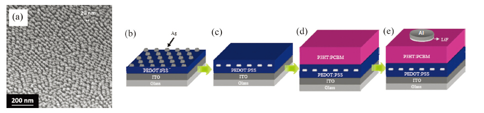
Plasmonic nanoparticle arrays can be prepared using NIL-based process. Different with other approaches utilizing non-regular nanoparticles,NIL-based nanoparticle fabrication process has advantages such as easy controllability of dimension and high uniformity in large-area format [48]. To prepare large-area and uniform metallic nanostructures,elastomeric stamps having dense 20 nm nanodot patterns,based on high modulus PDMS [49],were fabricated using SiO2 hole type mold (Fig. 3). Fabrication procedures of SiO2 hole type mold,based on self-assembled block copolymer template,are described elsewhere [50]. Using an angled deposition of metal onto the PDMS nanodot structures,highdensity sub-20 nm size Ag plasmonic nanostructures,expected to work as local field enhancer,were successfully fabricated (Fig. 4a). The position and the magnitude of extinction of peak,related to the localized surface plasmon resonance (LSPR),can be tunable by changing the thickness of the metal [50],similar to that reported by Lucas et al. [48].

|
Download:
|
| Fig. 3. (a) SEM of Ag plasmonic nanodot arrays deposited on nanodot type PDMS stamp using angled deposition,(b)-(e) fabrication procedures of normal configuration OPV cell with Ag plasmonic nanodot arrays. | |

|
Download:
|
| Fig. 4. Schematic of the process for fabricating plasmonic nanodot arrays: (a) SiO2 nanohole type structure; (b) nanodot soft stamp; (c) plasmonic metal nanodots. | |
Ag nanostructures formed on soft PDMS stamp or hard SiO2 mold,treated by fluoro-surfactant,could be efficiently transferred to PEDOT:PSS layer that could be used as HTL of normal configuration OPV (Fig. 4b). Thin PEDOT:PSS was further casted to restrict direct contact between metal nanoparticles and photoactive layer,leading to quenching of generated excitions (Fig. 4c). After spin-casting P3HT:PCBM blend for BHJ photoactive layer (Fig. 4d),LiF and Al were thermally deposited as a cathode electrode (Fig. 4e). As shown in Fig. 5,photoactive layer shows the improved absorption with Ag plasmonic nanodot array,and increased power conversion efficiency (PCE) (from 3.31% to 3.66%),originated by improved short circuit current (from 8.53 mA cm-2 to 9.58 mA cm-2),was obtained.

|
Download:
|
| Fig. 5. (a) Absorption spectra of photoactive layer with and without plasmonic Ag nanodot arrays. (b) J-V plot of OPV cells with and without plasmonic Ag nanodot arrays (with Ag: Jsc = 9.58 mA cm-2,Voc = 0.60 V,FF = 63.5%,PCE = 3.66%,without Ag: Jsc = 8.53 mA cm-2,Voc = 0.62 V,FF = 62.6%,PCE = 3.31%). | |
Periodic nanostructures such as nanogratings that can easily control the geometrical parameters are also applicable to OPV cells to manage the light in the device structures [1, 29, 30, 51, 52]. For example,it has been demonstrated that Ag nanograting,embedded in PEDOT:PSS buffer layer,can enhance the absorption of incident light by SPR and waveguide effect,giving 40% improved short circuit current and 2.5 fold enhanced external quantum efficiency at a certain wavelength (Fig. 6) [11]. Consequently about 35% improved PCE was achieved using phthalocyanine (CuPc) and C60 as donor and acceptor,respectively. In this work,metal nanograting structure was also utilized as transparent electrode that can substitute ITO electrode.

|
Download:
|
| Fig. 6. (a) Schematic of the fabricated small molecular weight OPV cell. The fabricated devices have the layered structure of Ag nanowire anode,PEDOT:PSS,CuPc,C60,BCP,and cathode (thick Ag film) from bottom to top. (b) Cross-sectional view of one of the fabricated devices,but without 70 nm thick Ag cathode. Organic materials have the sinusoidal shape due to the height profile of the Ag nanowire array and the nature of thermal evaporation process. Organic layers are depicted with solid lines and the square shows the position of the Ag nanowire on glass substrate. The scale bar is 200 nm. (c) J-V curve of the nanowire and control ITO devices. (d) External quantum efficiencies (EQE) enhancement of nanowire device with reference to ITO device. The inset gives the measured EQE of the nanowire and ITO devices. Reproduced with permission [11]. Copyright 2010,Wiley. | |
Metal nanogratings on OPV cells as light-trapping structure were also studied. By adding periodic nanostructure at the interface between photoactive layer and metal electrode,also working as reflector in OPV,the optical path length across a broad wavelength range of incident light could be enhanced. Periodic nanostructures could be easily introduced by printing photoactive layer,before the film is fully dried after spin-casting,with nanopattened PDMS stamp. After releasing the stamp,further metal deposition for electrode completed the light-trapping nanograting structure at the interface between metal and dielectric materials.
Fig. 7a shows SiO2 nanograting,utilized to fabricate PDMS stamp. The calculated enhancement effects of absorption after introducing the metal nanograting structure are shown in Fig. 7b, and the experimental results are demonstrated in Fig. 7c and d. The designed structure was 700 nm period metal nanograting having 350 nm line width. According to the calculation,the absorption enhancement in P3HT:PCBM system with those nanostructures was 2.71-fold (TM: 3.08,TE: 2.34) and this enhancement was expected to increase the short-circuit current (Jsc) without changing other factors. As expected,the real device fabricated using this structure showed the increased Jsc (from 8.84 to 10.85 mA cm-2) and external quantum efficiency (EQE). Consequently, the PCE was improved from 3.36% to 4.16%.

|
Download:
|
| Fig. 7. (a) SiO2 nanogratings,utilized to fabricate PDMS stamp. (b) Calculated absorption of light with and without light trapping structure. TE and TM waves mean transverse electric and transverse magnetic waves,respectively. The polarized light having the E-field parallel to the nanograting direction is defined as TE and the polarized light having E-field perpendicular to the nanograting direction is defined as TM. (c) J-V plots of OPV cells with and without nanogratings (with: Jsc = 10.85 mA cm-2,Voc = 0.60 V, FF = 63.8%,PCE = 4.16%,without: Jsc = 8.84 mA cm-2,Voc = 0.60 V,FF = 63.2%,PCE = 3.36%). (d) External quantum efficiency spectra of OPVs with and without nanogratings. | |
While most researchers in the field are exploiting plasmonic enhanced PV structures by matching the SPP resonance to the peak absorption of the semiconductor material,we think this strategy is only valid for very thin layer of active materials where light at peak absorption wavelength still cannot be absorbed completely in the round trip in the thin layer. Under the normal device construction where the thickness is optimized so that light can be absorbed efficiently at peak absorption,adding plasmonic particles would actually degrade the device performance as the particles themselves could also have strong absorption. In this case,we believe it is more desirable to have the SPP resonance wavelength to locate at the weak absorption range of the organic semiconductor,so that it can boost the absorption of the material,and lead to overall higher photocarrrier generation. In fact,the periodic structures described in Section 5 have the plasmonic peak at the wavelength range where the organic semiconductors absorb weakly,which may explain the overall 35% improvement in the PCE [11].
The absorption effect also depends on the particle size. For example,scattering dominates for particles sizes greater than 50 nm while absorption dominates for smaller particles. Therefore larger particles are desirable for light scattering and light trapping, and they can efficiently enhance the absorption of light in buffer layer as well as photoactive layer. However,as for smaller nanoparticles (<20 nm) case,because the field enhancement is localized around those nanoparticles and decay quickly with distance from the surface,embedding them to photoactive layer is more efficient than adding them to buffer layer. On the other hand, those nanoparticles in photoactive layer can act as recombination site of photogenerated excitons. To prevent this,the interface between nanoparticle and organic semiconductor needs to be controlled by treating the surface of nanoparticles (e.g.with thin insulating layer),however,the thickness of the additional layer also should be considered not to degrade the optical enhancement effect.
Furthermore,one also needs to consider that the metal nanostructures do not cause issues in excessive film roughness that could also degrade the device performance. Because the thicknesses of organic semiconductor thin films in OPV are usually tens of nanometer scale,the existence of additional nanostructure in those layers affects the morphologies of the films. For example, as shown in Fig. 6,metal nanogratings in HTL induce the sinusoidal shape device architecture and,in worst case,this structure can induce shunt pathway reducing the fill factor of PV cells. Therefore, the effect of morphological change,originated from the nanostructure, on the performances of OPV cells should be clarified to maximize the optical enhancement effect. 7. Conclusion
Metal nanostructures incorporated in buffer layer or photoactive layer of OPV cells can affect optical properties as well as electrical properties of the OPV devices. By choosing proper organic semiconductors and adjusting the dimension of metal nanostructures such that SP enhanced spectral range matches the peak absorption of organic semiconductor,further enhanced PCEs are expected. Another approach is to have peak enhancement of the metallic structure to match the low absorption range of the organic semiconductor and to significantly enhance the light absorption in this range. Therefore,the size and shape of plasmonic nanostructures and device architectures with structures,affecting extinction wavelength and absorption/scattering behavior of plasmonic nanostructures,should be precisely designed to utilize plasmonic optical enhancement to OPV devices.
AcknowledgmentsLJG acknowledges the partial support of this work by NSF and KAUST. HJP acknowledges the partial support by the Basic Science Research Program through the National Research Foundation of Korea (NRF) funded by the Ministry of Education (No. 2014R1A1A2056403). The authors would like to thank Dr. Ting Xu at National Institute of Standards and Technology for help with optical calculation for metal nanograting structure.
| [1] | H.A. Atwater, A. Polman, Plasmonics for improved photovoltaic devices, Nat. Mater. 9 (2010) 205-213. |
| [2] | E. Ozbay, Plasmonics: merging photonics and electronics at nanoscale dimensions, Science 311 (2006) 189-193. |
| [3] | W.L. Barnes, A. Dereux, T.W. Ebbesen, Surface plasmon subwavelength optics, Nature 424 (2003) 824-830. |
| [4] | X.G. Luo, T. Ishihara, Surface plasmon resonant interference nanolithography technique, Appl. Phys. Lett. 84 (2004) 4780-4782. |
| [5] | N. Fang, H. Lee, C. Sun, X. Zhang, Sub-diffraction-limited optical imaging with a silver superlens, Science 308 (2005) 534-537. |
| [6] | M.G. Albrecht, J.A. Creighton, Anomalously intense Raman spectra of pyridine at a silver electrode, J. Am. Chem. Soc. 99 (1977) 5215-5217. |
| [7] | H.J. Park, T. Xu, J.Y. Lee, A.B. Ledbetter, L.J. Guo, Photonic color filters integrated with organic solar cells for energy harvesting, ACS Nano 5 (2011) 7055-7060. |
| [8] | T.H. Reilly III, J. van de Lagemaat, R.C. Tenent, A.J. Morfa, K.L. Rowlen, Surface plasmon enhanced transparent electrodes in organic photovoltaics, Appl. Phys. Lett. 92 (2008) 243304. |
| [9] | S.-W. Baek, J. Noh, C.-H. Lee, et al., Plasmonic forward scattering effect in organic solar cells: a powerful optical engineering method, Sci. Rep. 3 (2013) 1726. |
| [10] | L.Y. Lu, Z.Q. Luo, T. Xu, L.P. Yu, Cooperative plasmonic effect of Ag and Au nanoparticles on enhancing performance of polymer solar cells, Nano Lett. 13 (2013) 59-64. |
| [11] | M.-G. Kang, T. Xu, H.J. Park, X. Luo, L.J. Guo, Efficiency enhancement of organic solar cells using transparent plasmonic Ag nanowire electrodes, Adv. Mater. 22 (2010) 4378-4383. |
| [12] | M.-G. Kang, H.J. Park, S.H. Ahn, T. Xu, L.J. Guo, Toward low-cost, high-efficiency, and scalable organic solar cells with transparent metal electrode and improved domain morphology, IEEE J. Sel. Top. Quantum Electron. 16 (2010) 1807-1820. |
| [13] | H.J. Park, M.-G. Kang, S.H. Ahn, L.J. Guo, A facile route to polymer solar cells with optimum morphology readily applicable to a roll-to-roll process without sacrificing high device performances, Adv. Mater. 22 (2010) E247-E253. |
| [14] | H.J. Park, H. Kim, J.Y. Lee, T. Lee, L.J. Guo, Optimization of polymer photovoltaic cells with bulk heterojunction layers hundreds of nanometers thick: modifying the morphology and cathode interface, Energy Environ. Sci. 6 (2013) 2203-2210. |
| [15] | H.J. Park, J.Y. Lee, T. Lee, L.J. Guo, Advanced heterojunction structure of polymer photovoltaic cell generating high photocurrent with internal quantum efficiency approaching 100%, Adv. Energy Mater. 3 (2013) 1135-1142. |
| [16] | P.E. Shaw, A. Ruseckas, I.D.W. Samuel, Exciton diffusion measurements in poly(3- hexylthiophene), Adv. Mater. 20 (2008) 3516-3520. |
| [17] | W.A. Luhman, R.J. Holmes, Investigation of energy transfer in organic photovoltaic cells and impact on exciton diffusion length measurements, Adv. Funct. Mater. 21 (2011) 764-771. |
| [18] | M. Theander, A. Yartsev, D. Zigmantas, et al., Photoluminescence quenching at a polythiophene/C60 heterojunction, Phys. Rev. B 61 (2000) 12957-12963. |
| [19] | S.S. Kim, S.I. Na, J. Jo, D.Y. Kim, Y.C. Nah, Plasmon enhanced performance of organic solar cells using electrodeposited Ag nanoparticles, Appl. Phys. Lett. 93 (2008) 073307. |
| [20] | M. Iqbal, Y.I. Chung, G. Tae, An enhanced synthesis of gold nanorods by the addition of Pluronic (F-127) via a seed mediated growth process, J. Mater. Chem. 17 (2007) 335-342. |
| [21] | H.A. Day, D. Bartczak, N. Fairbairn, et al., Controlling the three-dimensional morphology of nanocrystals, Cryst. Eng. Commun. 12 (2010) 4312-4316. |
| [22] | F.C. Chen, J.L. Wu, C.L. Lee, et al., Plasmonic-enhanced polymer photovoltaic devices incorporating solution-processable metal nanoparticles, Appl. Phys. Lett. 95 (2009) 013305. |
| [23] | J.H. Lee, J.H. Park, J.S. Kim, D.Y. Lee, K. Cho, High efficiency polymer solar cells with wet deposited plasmonic gold nanodots, Org. Electron. 10 (2009) 416-420. |
| [24] | E. Stratakis, M. Barberoglou, C. Fotakis, et al., Generation of Al nanoparticles via ablation of bulk Al in liquids with short laser pulses, Opt. Express 17 (2009) 12650-12659. |
| [25] | A.J. Morfa, K.L. Rowlen, T.H. Reilly III, M.J. Romero, J.V.D. Lagemaat, Plasmonenhanced solar energy conversion in organic bulk heterojunction photovoltaics, Appl. Phys. Lett. 92 (2008) 013504. |
| [26] | C.F. Bohren, D.R. Huffman, Absorption and Scattering of Light by Small Particles, Wiley-Interscience, New York, USA, 1983. |
| [27] | G. Spyropoulos, M. Stylianakis, E. Stratakis, E. Kymakis, Organic bulk heterojunction photovoltaic devices with surfactant-free Au nanoparticles embedded in the active layer, Appl. Phys. Lett. 100 (2012) 213904. |
| [28] | S. Pillai, K.R. Catchpole, T. Trupke, M.A. Green, Surface plasmon enhanced silicon solar cells, J. Appl. Phys. 101 (2007) 093105. |
| [29] | M.A. Sefunc, A.K. Okyay, H.V. Demir, Plasmonic backcontact grating for P3HT:PCBM organic solar cells enabling strong optical absorption increased in all polarizations, Opt. Express 19 (2011) 14200-14209. |
| [30] | M.G. Kang, H.J. Park, S.H. Ahn, L.J. Guo, Transparent Cu nanowire mesh electrode on flexible substrates fabricated by transfer printing and its application in organic solar cells, Sol. Energy Mater. Sol. Cells 94 (2010) 1179-1184. |
| [31] | J.L. Wu, F.C. Chen, Y.S. Hsiao, et al., Surface plasmonic effects of metallic nanoparticles on the performance of polymer bulk heterojunction solar cells, ACS Nano 5 (2011) 959-967. |
| [32] | J.N. Pei, J.L. Tao, Y.H. Zhou, et al., Efficiency enhancement of polymer solar cells by incorporating a self-assembled layer of silver nanodisks, Sol. Energy Mater. Sol. Cells 95 (2011) 3281-3286. |
| [33] | L.F. Qiao, D. Wang, L.J. Zuo, et al., Localized surface plasmon resonance enhanced organic solar cell with gold nanospheres, Appl. Energy 88 (2011) 848-852. |
| [34] | Y.S. Hsiao, S. Charan, F.Y. Wu, et al., Improving the light trapping efficiency of plasmonic polymer solar cells through photon management, J. Phys. Chem. C 116 (2012) 20731-20737. |
| [35] | H. Choi, S.J. Ko, Y. Choi, et al., Versatile surface plasmon resonance of carbon-dotsupported silver nanoparticles in polymer optoelectronic devices, Nat. Photonics 7 (2013) 732-738. |
| [36] | J. Yang, J. You, C.C. Chen, et al., Plasmonic polymer tandem solar cell, ACS Nano 5 (2011) 6210-6217. |
| [37] | D.D.S. Fung, L. Qiao, W.C.H. Choy, et al., Optical and electrical properties of efficiency enhanced polymer solar cells with Au nanoparticles in a PEDOT-PSS layer, J. Mater. Chem. 21 (2011) 16349-16356. |
| [38] | M. Stavytska-Barba, A.M. Kelley, Surface-enhanced Raman study of the interaction of PEDOT:PSS with plasmonically active nanoparticles, J. Phys. Chem. C 114 (2010) 6822-6830. |
| [39] | D.H. Wang, D.Y. Kim, K.W. Choi, et al., Enhancement of donor-acceptor polymer bulk heterojunction solar cell power conversion efficiencies by addition of Au nanoparticles, Angew. Chem. Int. Ed. 50 (2011) 5519-5523. |
| [40] | D.H. Wang, K.H. Park, J.H. Seo, et al., Enhanced power conversion efficiency in PCDTBT/PC70BM bulk heterojunction photovoltaic devices with embedded silver nanoparticle clusters, Adv. Energy Mater. 1 (2011) 766-770. |
| [41] | C.H. Kim, S.H. Cha, S.C. Kim, et al., Silver nanowire embedded in P3HT:PCBM for high-efficiency hybrid photovoltaic device applications, ACS Nano 5 (2011) 3319- 3325. |
| [42] | D.H. Wang, J.K. Kim, G.-H. Lim, et al., Enhanced light harvesting in bulk heterojunction photovoltaic devices with shape-controlled Ag nanomaterials: Ag nanoparticles versus Ag nanoplates, RSC Adv. 2 (2012) 7268-7272. |
| [43] | K. Topp, H. Borchert, F. Johnen, et al., Impact of the incorporation of Au nanoparticles into polymer/fullerene solar cells, J. Phys. Chem. A 114 (2010) 3981-3989. |
| [44] | M.D. Brown, T. Suteewong, R.S.S. Kumar, et al., Plasmonic dye-sensitized solar cells using core-shell metal-insulator nanoparticles, Nano Lett. 11 (2010) 438-445. |
| [45] | H.C. Liao, C.S. Tsao, T.H. Lin, et al., Nanoparticle-tuned self-organization of a bulk heterojunction hybrid solar cell with enhanced performance, ACS Nano 6 (2012) 1657-1666. |
| [46] | B. Paci, G.D. Spyropoulos, A. Generosi, et al., Enhanced structural stability and performance durability of bulk heterojunction photovoltaic devices incorporating metallic nanoparticles, Adv. Funct. Mater. 21 (2011) 3573-3582. |
| [47] | B. Paci, A. Generosi, V.R. Albertini, et al., Enhancement of photo/thermal stability of organic bulk heterojunction photovoltaic devices via gold nanoparticles doping of the active layer, Nanoscale 4 (2012) 7452-7459. |
| [48] | B.D. Lucas, J. Kim, C. Chin, L.J. Guo, Nanoimprint lithography based approach for the fabrication of large-area, uniformly-oriented plasmonic arrays, Adv. Mater. 20 (2008) 1129-1134. |
| [49] | C. Pina-Hernandez, J.S. Kim, L.J. Guo, P.F. Fu, High-throughput and etch-selective nanoimprinting and stamping based on fast-thermal-curing poly(dimethylsiloxane) s, Adv. Mater. 19 (2007) 1222-1227. |
| [50] | H.J. Park, M.G. Kang, L.J. Guo, Large area high density sub-20 nm SiO2 nanostructures fabricated by block copolymer template for nanoimprint lithography, ACS Nano 3 (2009) 2601-2608. |
| [51] | K. Tvingstedt, N.K. Persson, O. Inganas, A. Rahachou, I.V. Zozoulenko, Surface plasmon increase absorption in polymer photovoltaic cells, Appl. Phys. Lett. 91 (2007) 113514. |
| [52] | C. Min, J. Li, G. Veronis, et al., Enhancement of optical absorption in thin-film organic solar cells through the excitation of plasmonic modes in metallic gratings, Appl. Phys. Lett. 96 (2010) 133302. |