


b State Key Laboratory of Solid Lubrication, Lanzhou Institute of Chemical Physics, Chinese Academy of Sciences, Lanzhou 730000, China
Usually,complexing agents are used to enhance the uniformity and quality of thin films in the chemical bath deposition technique [23, 24]. Moreover,some physical and chemical properties of materials are dependent on the complexing agents [25]. Singh et al.[26] reported the influence of complex agent on both conversion efficiency and stability to degradation of bath deposited CdS photoelectrode under PEC conditions. Cheng investigated the structural,electrical,and optical properties of the Ag-In-S ternary system semiconductor using the method of CBD. The results showed that the complexing agents in the solution played important roles in the nucleation and growth of thin films [27]. In addition,the absorbed ligands can change the growth kinetics and surface energies of different crystal faces,which will lead to anisotropic growth of low symmetry nanostructures and further produce nanoparticles of different morphology,such as nanorods,nanodisks and nanowires [28].
No matter whether a film or other nanostructure of Cu2-xS,the difficulties in composition control and product impurity levels are the common challenges of methods mentioned above. In the present work,Cu2-xS (x = 0,1) thin films were successfully synthesized on the self-assembled,monolayer substrate with various concentrations of complexing agents in the solution using the chemical bath deposition (CBD) method. The effects of the concentration of the complexing agent on crystal structure,optical properties and photo-electrochemical response of nanostructured Cu2-xS thin films were investigated by XRD,UV-vis spectrum and computer controlled potentiostat (CHI 660d) with a threeelectrode system. The growth mechanisms of Cu2-xS nanocrystals with different EDTA concentrations are proposed and discussed as well. This paper also demonstrates some of the existing uncertainties about the physical-chemical properties of Cu2-xS with different chemical stoichiometries. 2. Experimental 2.1. Preparation of Cu2-xS thin films
The procedure for preparation of SAMs with -NH2 terminal groups has been detailed in our previous work [29]. To ensure successful preparation of SAMs,the static contact angles of water on SAMs were 50-52° (-NH2 terminal group),in agreement with the literature [30].
The Cu2-xS thin films were prepared by a simple chemical bath deposition method. The functionalized substrates were immersed in a prepared precursor solution consisting of 10 mmol/L CuSO4·5H2O (copper source),10 mmol/L Na2S2O3 (sulfur source) and EDTA (complexing agent) with different molar ratio w = 0.5,1.5 and 3 (molar ratio between EDTA and CuSO4·5H2O),which were labeled as S1,S2 and S3,respectively. The solution temperature was maintained at 70 ℃ using a thermostatically controlled water bath. The pH of the bath solution was adjusted to 2.3 by adding H2SO4 solution (1 mol/L). After deposition,the deposited films were rinsed in deionized water and ultrosonicated to remove any leftover Cu2-xS precipitates,and finally,dried with nitrogen gas. 2.2. Characterization
The structure and the phase composition were analyzed by X’pert PRO X-ray diffraction (XRD,Netherlands) with Cu Kα radiation at the scanning speed of 1.2°/min. The chemical states of the elements on the films were determined using a PHI5702 multifunctional X-ray photoelectron spectroscope (XPS,USA). The XPS analysis was conducted at 400W and pass energy of 29.35 eV,using AlKα (1486.6 eV) radiation as the excitation source and the binding energy of contaminated carbon (C 1s = 284.6 eV) as reference. Field emission scanning electron microscopy (FESEM,JSM-5600LV,Japan) and transmission electron microscopy (TEM) were used to study the surface morphology of the thin films. The optical absorption spectra were obtained with a UV-vis spectrophotometer (U-3010,Japan) within the wavelength range of 300- 1000 nm. A computer controlled potentiostat (CHI 660d) was used for all PEC experiments. The PEC responses of the samples were measured in an electrochemical cell with a three-electrode system,in which Cu2-xS thin films,a platinum wire and saturation mercury electrode were used as the working electrode,the counter electrode and reference electrode,respectively. A 125W mercury lamp was used as the light source. The electrolyte,aqueous HClO4 (0.1 mol/L) solutions,was freshly prepared using double deionized water. Then,the electrolyte was put into an ultrasonic bath for 30 min before each experiment in order to decrease the gas solutes in the electrolytes. 3. Results and discussion 3.1. Films formed on APTS SAMs
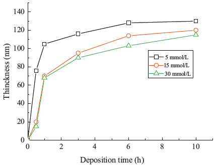
The nucleation and growth of thin films are affected by the degree of super saturation that can be controlled by varying solution conditions. In this research,the effects of EDTA concentration on the nucleation and growth of Cu2-xS films were examined in detail. Fig. 1 shows the growth rate of Cu2-xS films on the substrate at different EDTA:Cu2+ ratios. It shows that after the induction period,the film growth is initially linear with time followed by a nonlinear region of a much lower growth rate. The decrease of the EDTA concentration resulted in a higher growth rate and shorter inducing time. The thickness of samples S1,S2 and S3 on the substrate with APTS SAMs nearly reached a maximum after 6 h,9 h and 10 h in the solution at 70℃,respectively.

|
Download:
|
| Fig. 1. The thickness of films on the substrate as a function of the deposition time,the open squares,circles,and triangles represent the films with final thickness of 132 nm,120 nm,and 115 nm,respectively. | |
Fig. 2 presents the XRD patterns of samples S1,S2,and S3. The as-prepared samples consisting of copper sulfide nanocrystals were confirmed by XRD pattern. The peaks of S1 (Fig. 2a) can match the orthorhombic Cu2S crystal phase with a = 11.73Å ,b = 27.1Å and c = 22.67Å ,which matches the JCPDS reference file for Cu2S [02-1294]. Therefore,at w = 0.5,it consists of well-defined diffraction peaks of cuprous sulfide,indicating that pure Cu2S thin film is formed onto the Si substrate. Samples S2 and S3,however,show the diffraction pattern of hexagonal CuS (No. 01-1281) crystal phase with a = 3.800Å and a = 16.33Å for S2 (Fig. 2b) and a = 3.787Å and c = 16.44Å for S3 (Fig. 2c). The board peak at 56° should be assigned to the Si substrate. The diffraction pattern also revealed that the crystallinity is slightly preferred for S3,as the peak intensity is higher compared with the other two samples. It is attributed to slow precipitation of the CuS molecules (as shown in Fig. 1),which is caused by relatively high concentration of EDTA complex. XPS spectrums of Cu 2p for the samples (S1,S2 and S3) are shown in Fig. 3. In Fig. 3a,the binding energies of the observed photoelectron peaks of Cu 2p3/2,2p1/2 for Cu2S were 932.8 eV and 952.7 eV,respectively. In Fig. 3b and c,the binding energies of the observed photoelectron peaks of Cu 2p3/2,2p1/2 for CuS were 932.3 eV and 952.2 eV,and were well consistent with the standard reference XPS spectrum of Cu 2p in CuS. It can be calculated that the Cu/S ratio is 1.9922 and 0.9835 for Cu2S and CuS,respectivel.

|
Download:
|
| Fig. 2. XRD patterns of copper sulfide thin films formed with different EDTA:Cu2+ratios: (a) 0.5:1,(b) 1.5:1 and (c) 3:1 at 70 ℃ | |

|
Download:
|
| Fig. 3. XPS (Cu2p region) of Cu2S and CuS with different the molar ratio between EDTA and Cu2+: (a) 0.5:1,(b) 1.5:1 and (c) 3:1. | |

|
Download:
|
| Fig. 4. FESEM images of copper sulfide thin film formed with EDTA:Cu2+ ratio of (a) 0.5:1,(b) 1.5:1 and (c) 3:1 at 70 ℃. | |

|
Download:
|
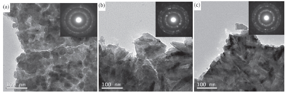
| Fig. 5. TEM images of copper sulfide thin film formed with EDTA:Cu2+ ratio of (a) 0.5:1,(b) 1.5:1 and (c) 3:1 at 70 ℃. Inset: the corresponding SAED patterns. | |
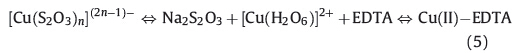
The deposition process is based on slow release of Cu2+ and S2- ions. The free copper and sulfide ion must be maintained at low concentration in order to avoid the process of immediate precipitation. In the present case,sulfide ions are generated in the bath from sodium thiosulfate,as shown below:


Na2S2O3 is reducing agent by virtue of the half cell reaction [32]. In the acidic medium of pH 2.3,sodium thiosulfate gradually release sulfide ions upon hydrolytic decomposition [33]. The copper salt is dissolved in deionized distilled water to form [Cu(H2O)6]2+ ions,and by adding the ligand to this solution leads to the formation of complexes by successive displacement of water molecules. However,there exists an equilibrium between the Cu(II) and Cu(I) oxidation states [5];

The relative stability of Cu(I) and Cu(II) depends upon the nature of anion or ligand in the bath. In this technique,the thiosulfate ions can also be used as a complexing agent. Copper is known to form at least three consecutive complex compounds with the thiosulfate: [Cu(S2O3)n]-,[Cu(S2O3)n]3-,[Cu(S2O3)n]5- [33]. Therefore,there exists the following equilibrium,
At w = 0.5,due to lower concentration of EDTA,Cu(II) in cupric sulfide tend to be reduced and combined with thiosulfate to form anionic thiosulfatecopper(I) complex compound,[Cu(S2O3)n]-. The dissociation of this gives Cu(I) ions,[Cu(S2O3)n]-⇔Cu+ (aq.) + n(S2O3)2- [34]. The cuprous ions then combine with the sulfide ions,to form insoluble Cu2S. However,at w = 1.5 and higher ratios up to 3,due to the excessive concentration of EDTA,Cu(II) firstly combines with the EDTA and forms the Cu(II)-EDTA complex. Then,the EDTA complex breaks down slowly with temperature releasing the Cu(II) ions,which will react finally with sulfide ion to form a CuS thin film. Therefore,the control of the crystal structure of the Cu2-xS has been realized by utilizing different concentrations of complexing agent during chemical bath deposition. 3.4. Optical and photoelectrochemical properties
UV-vis absorptions of Cu2-xS thin films with different concentrations of EDTA were investigated to examine the effects of the morphology and structure on the optical properties. As shown in Fig. 6,the absorption edge of the thin film varies with composition ‘‘x’’. The absorption spectrum of sphere-like Cu2S nanocrystals (w = 0.5),exhibits a well-defined absorption feature at 365 nm and has a broad absorption between 450 and 650 nm,which is also the most important reason for their applications in solar energy adsorption and photovoltaic devices [35]. On the other hand,the absorbance never reaches zero intensity,but rises for longer wavelengths again,which is thought to be caused by the free-carrier intraband absorbance. Therefore,samples prepared were assigned to Cu2S nanocrytals. It shows that the spectrum of CuS thin film (w = 1.5 and 3) has a strong absorption around 396 and 400 nm (Fig. 6b and c),which has red-shift compared with Cu2S thin film due to the quantum size effect,and reaches a minimum around 550 nm,but again does not decrease to zero intensity. It rises for longer wavelengths stronger than the Cu2S,which is attributed to free-carrier absorbance [8].

|
Download:
|
| Fig. 6. The optical absorption spectra of the samples: (a) S1,(b) S2 and (c) S3. | |
The photoelectrochemical (PEC) responses of the samples were measured to examine the possibility of their application in solar energy cells [26, 36]. In Fig. 7,instantaneous photoresponse of the three samples were featured with the rise and decay curves of photocurrent (Isc) during successive exposure of the films to illuminated and dark conditions. It can be seen that all samples have very intense photocurrent responses when the light was regularly switched ‘‘on’’ and ‘‘off’’,a series of almost identical electric signals can be obtained and hold the stable photocurrent. For the Cu2-xS thin films with different w values (0.5,1.5,3),Isc were ca. 0.204,0.084,and 0.09 A/m2,respectively. The Cu2S (w = 0.5) shows the higher value of generated photocurrents compared with that of CuS (w = 1.5 and 3). On the one hand,the Cu2S is appealing as an absorber layer in thin film photovoltaics due to the nearly ideal bandgap. On the other hand,this was attributed to the high density of the copper vacancies of Cu2S as it was proposed that the density of the copper vacancies increased with the increment of 2-x value for the Cu2-xS thin films [37].

|
Download:
|
| Fig. 7. The plot of Isc versus time (a) S1,(b) S2 and (c) S3. The illumination was alternately on and off for 5 s. 4. Conclusion | |
In this study,the Cu2-xS (x = 0,1) semiconductor films were successfully deposited using chemical bath deposition. The structural,optical and photoelectrochemical properties of Cu2-xS thin films were investigated. With an increase of the concentration of the complexing agent EDTA in the reaction solution,it was found that the compositions of the Cu2-xS nanocrystals were varied from Cu2S (chalcocide) to CuS (covellite). Moreover,the high concentration of EDTA led to better crystallinity and sheetlikemorphology. A UV-vis absorption analysis illustrated that the maximum in the absorption spectra of Cu2-xS (x = 0,1)films shifts to longer wavelength with an increase of the concentration of EDTA in the solution. According to experimental results,all samples showed a photo-enhancement effect. The photocurrent density of Cu2S thin film reached 0.204 A/m2 at the external potential of -0.6 V versus a Pt electrode,which showed that Cu2S thin film can be used as a good photo-absorber in PEC applications.
| [1] | D.C. Reynolds, G. Leies, L.L. Antes, R.E. Marburger, Photovoltaic effect in cadmium sulfide, Phys. Rev. 96 (1954) 533-534. |
| [2] | Y.B. Li, W. Lu, Q. Huang, et al., Copper sulfide nanoparticles for photothermal ablation of tumor cells, Nanomedicine 5 (2010) 1161-1171. |
| [3] | I. Ancutiene, V. Janickis, R. Ivanauskas, Formation and characterization of conductive thin layers of copper sulfide (CuxS) on the surface of polyethylene and polyamide by the use of higher polythionic acids, Appl. Surf. Sci. 252 (2006) 4218-4225. |
| [4] | Z.B. Hai, J.L. Huang, H. Remita, J.F. Chen, Enhancement of alternating current electroluminescence properties by the addition of graphene oxide nanosheets as dielectric materials, Mater. Lett. 108 (2013) 304-307. |
| [5] | M.T.S. Nair, L. Guerrero, P.K. Nair, Conversion of chemically deposited CuS thin films to Cu1.8S and Cu1.96S by annealing, Semicond. Sci. Technol. 13 (1998) 1164-1169. |
| [6] | C. Nunes de Carvalho, P. Parreira, et al., P-type CuxS thin films: integration in a thin film transistor structure, Thin Solid Films 543 (2013) 3-6. |
| [7] | H.T. Zhu, J.X. Wang, D.X. Wu, Fast synthesis, formation mechanism, and control of shell thickness of CuS hollow spheres, Inorg. Chem. 48 (2009) 7099-7104. |
| [8] | Y. Zhao, H. Pan, Y. Lou, et al., Plasmonic Cu2-xS nanocrystals: optical and structural properties of copper-deficient copper(I) sulfides, J. Am. Chem. Soc. 131 (2009) 4253-4261. |
| [9] | P. Kumar, M. Gusain, R. Nagarajan, Synthesis of Cu1.8S and CuS from copperthiourea containing precursors; anionic (Cl , NO3 , SO4 2 ) influence on the product stoichiometry, Inorg. Chem. 50 (2011) 3065-3070. |
| [10] | Q. Tian, M. Tang, Y. Sun, et al., Hydrophilic flower-like CuS superstructures as an efficient 980 nmlaser-driven photothermal agent for ablation of cancer cells, Adv. Mater. 23 (2011) 3542-3547. |
| [11] | N. Banerjee, S.B. Krupanidhi, Synthesis and structural characterization of two dimensional hierarchical covellite nano-structures, Mater. Chem. Phys. 137 (2012) 466-471. |
| [12] | S. Xu, Q. Wang, J.H. Cheng, Q.H. Meng, Y. Jiao, Preparation and characteristics of porous CuS microspheres consisted of polycrystalline nanoslices, Powder Technol. 199 (2010) 139-143. |
| [13] | M. Saranya, C. Santhosh, R. Ramachandran, et al., Hydrothermal growth of CuS nanostructures and its photocatalytic properties, Powder Technol. 252 (2014) 25-32. |
| [14] | J. Li, T.G. Jiu, G.H. Tao, et al., Manipulating surface ligands of copper sulfide nanocrystals: synthesis, characterization, and application to organic solar cells, J. Colloid Interface Sci. 419 (2014) 142-147. |
| [15] | M. Kemmler, M. Lazell, P. O'Brien, et al., The growth of thin films of copper chalcogenide films by MOCVD and AACVD using novel single-molecule precursors, J. Mater. Sci. Mater. Electron. 13 (2002) 531-535. |
| [16] | R. Kobayashi, T. Wada, S. Bakehe, R. Klenk, The effect of sulphur pressure on the depth distribution of elements in Cu(In,Ga)S2 films, Thin Solid Films 472 (2005) 71-75. |
| [17] | R. Cordova, H. Gomez, R. Schrebler, et al., Electrosynthesis and electrochemical characterization of a thin phase of CuxS (x! 2) on ITO electrode, Langmuir 18 (2002) 8647-8654. |
| [18] | M.T.S. Nair, P.K. Nair, Chemical bath deposition of CuxS thin films and their prospective large area applications, Semicond. Sci. Technol. 4 (1989) 191-199. |
| [19] | K.M. Gadave, C.D. Lokhande, Formation of CuxS films through a chemical bath deposition process, Thin Solid Films 229 (1993) 1-4. |
| [20] | T. Yamamoto, K. Tanaka, E. Kubota, K. Osakada, Deposition of copper sulfide on the surface of poly(ethylene terephthalate) and poly(vinyl alcohol) films in aqueous solution to give electrically conductive films Sxad, Chem. Mater. 5 (1993) 1352- 1357. |
| [21] | R.S. Mane, C.D. Lokhande, Chemical deposition method for metal chalcogenide thin films, Mater. Chem. Phys. 65 (2000) 1-31. |
| [22] | Z. Tao, T. Zhan, T. Zhou, X. Zhao, Z. Li, Synthesis, properties, and self-assembly of 2,3-bis(n-octyl) hexaazatriphenylene, Chin. Chem. Lett. 24 (2013) 453-456. |
| [23] | A.U. Ubale, Effect of complexing agent on growth process and properties of nanostructured Bi2S3 thin films deposited by chemical bath deposition method, Mater. Chem. Phys. 121 (2010) 555-560. |
| [24] | S.C. Liufu, L.D. Chen, Q. Yao, F.Q. Huang, In situ assembly of CuxS quantum-dots into thin film: a highly conductive p-type transparent film, J. Phys. Chem. C 112 (2008) 12085-12088. |
| [25] | S.R. Gadakh, C.H. Bhosale, Effect of concentration of complexing agent (tartaric acid) on the properties of spray deposited Sb2S3 thin films, Mater. Chem. Phys. 78 (2003) 367-371. |
| [26] | S.B. Patil, A.K. Singh, Effect of complexing agent on the photoelectrochemical properties of bath deposited CdS thin films, Appl. Surf. Sci. 256 (2010) 2884-2889. |
| [27] | K.W. Cheng, S.C. Wang, Effects of complex agents on the physical properties of Ag-In-S ternary semiconductor films using chemical bath deposition, Mater. Chem. Phys. 115 (2009) 14-20. |
| [28] | M.B. Sigman, A. Ghezelbash, T. Hanrath, et al., Solventless synthesis of monodisperse Cu2S nanorods, nanodisks, and nanoplatelets, J. Am. Chem. Soc. 125 (2003) 16050-16057. |
| [29] | Y.J. Lu, X. Meng, G.W. Yi, J.H. Jia, In situ growth of CuS thin films on functionalized self-assembled monolayers using chemical bath deposition, J. Colloid Interface Sci. 356 (2011) 726-733. |
| [30] | N. Faucheux, R. Schweiss, K. Lutzow, C. Werner, T. Groth, Self-assembled monolayers with different terminating groups as model substrates for cell adhesion studies, Biomaterials 25 (2004) 2721-2730. |
| [31] | Y.H. Chen, C.Y. Huang, F.D. Lai, et al., Electroless deposition of the copper sulfide coating on polyacrylonitrile with a chelating agent of triethanolamine and its EMI shielding effectiveness, Thin Solid Films 517 (2009) 4984-4988. |
| [32] | M.D. Xin, K.W. Li, H. Wang, Synthesis of CuS thin films by microwave assisted chemical bath deposition, Appl. Surf. Sci. 256 (2009) 1436- 1442. |
| [33] | I. Grozdanov, C.K. Barlingay, S.K. Dey, M. Ristov, M. Najdoski, Experimental study of the copper thiosulfate system with respect to thin-film deposition, Thin Solid Films 250 (1994) 67-71. |
| [34] | S.V. Bagul, S.D. Chavhan, R. Sharma, Growth and characterization of CuxS (x=1.0, 1.76, and 2.0) thin films grown by solution growth technique (SGT), J. Phys. Chem. Solids 68 (2007) 1623-1629. |
| [35] | J.J. Nairn, P.J. Shapiro, B. Twamley, et al., Preparation of ultrafine chalcopyrite nanoparticles via the photochemical decomposition of molecular single-source precursors, Nano Lett. 6 (2006) 1218-1223. |
| [36] | D. Chen, Y.F. Gao, G. Wang, et al., Surface tailoring for controlled photoelectrochemical properties: effect of patterned TiO2 microarrays, J. Phys. Chem. C 111 (2007) 13163-13169. |
| [37] | E. Elizalde, F. Rueda, On minority-carrier transport parameter determination in heterojunctions from spectral response measurements: the cases of chalcocite, djurleite and digenite, J Phys. D: Appl. Phys. 19 (1986) 1563-1574. |