 2018, Vol. 46
文章信息
- 郝欢欢, 刘晶冰, 李坤威, 汪浩, 严辉
- HAO Huan-huan, LIU Jing-bing, LI Kun-wei, WANG Hao, YAN Hui
- 拉曼光谱表征石墨烯结构的研究进展
- Research Progress on Characterization of Graphene Structure by Raman Spectroscopy
- 材料工程, 2018, 46(5): 1-10
- Journal of Materials Engineering, 2018, 46(5): 1-10.
- http://dx.doi.org/10.11868/j.issn.1001-4381.2016.001341
-
文章历史
- 收稿日期: 2016-09-10
- 修订日期: 2017-09-15


2. 中国标准化研究院, 北京 100142
2. China National Institute of Standardization, Beijing 100142, China
人们在理论上对石墨烯的研究最早始于20世纪60年代[1-2],在当时已预测出二维石墨烯片的电荷载体会表现得像一个无质量的狄拉克费米子并能够指导大多数其他碳材料的量子特性。然而,直到21世纪初,英国曼彻斯特大学的安德烈·盖姆和康斯坦丁·诺沃肖洛夫才通过微机械力剥离法成功制备出单层石墨烯[3],有关石墨烯的研究也因此迅速风靡全球。石墨烯是指一层密集地包裹在蜂巢晶体点阵上排列成二维结构的碳原子[4],是目前世界上公认的最薄、最强韧的材料。石墨烯可以翘曲成零维的富勒烯,也可以卷成一维的碳纳米管或者堆垛成三维的石墨,因此石墨烯是构成其他维数的石墨材料的基本单元[5]。由于石墨烯的独特结构使它拥有多样化的电子和光学性质,包括高本征载流子迁移率(2000cm2·V-1·s-1)、高导热系数(≈5000Wm-1·K-1)、高弹性模量(≈1.0TPa)和光学透过率(≈97.7%)以及半整数的量子霍尔效应[6-7],因而在电子器件、自旋电子学、透明导电电极和能源存储等领域备受关注[8-13]。
基于石墨烯强大的潜在应用市场,一种快速的、灵敏的、非破坏性的、可提供高分辨率的电子结构信息,并适用于实验室和公司大规模生产的理想表征工具必不可少。拉曼光谱分析仪满足了所有的这些需求。拉曼光谱是一种基于单色光的非弹性散射的光谱技术,一般源于激光与样品间的相互作用。自2006年安德烈·盖姆和康斯坦丁·诺沃肖洛夫首次记录了拉曼光谱对石墨烯的结构表征[14],拉曼光谱已成为最受欢迎的表征石墨烯的技术之一,同时,一直以来它也被广泛应用于富勒烯、碳纳米管和金刚石等多种碳的同素异形体的结构表征中[15-18]。由于石墨烯带隙的缺乏使所有入射波共振,所以拉曼光谱可以有效地表征样品的分子振动特性和电子性质[19-20]。另外,拉曼光谱还是探究石墨烯内部电子和声子相互作用的重要工具。拉曼光谱看似简单,一般只在1000~2000cm-1光谱区域内包含几个重要的特征峰和更高区域内的一些二阶峰,但谱峰的强度、位置和半峰宽的微小变化都与碳材料的结构信息相关[21]。例如,根据2D峰的形状和位置可以简单且有效地判别石墨烯的层数,而且石墨烯结构中电子和空穴的掺杂也会引起2D峰的红移或蓝移[22-23]。本论文主要综述了近年来国内外学者利用拉曼光谱在石墨烯结构表征中的研究进展。
1 拉曼光谱在石墨烯层数判定上的应用图 1为采用514nm波长激光激发时石墨烯与石墨的典型拉曼光谱[24]。两个最突出的特征峰G峰和2D峰分别位于1580cm-1和2700cm-1附近,而强度稍弱的两个峰D峰和D′峰分别位于1350cm-1和2450cm-1附近[25]见图 1(a)。G峰与布里渊区中心的双重简并声子模(横向光学支和纵向光学支)有关,具有E2g对称性[26]。D峰和2D峰产生于第一布里渊区的二级双共振拉曼散射过程,其中2D峰源于区域边界处面内横向光学支声子,而D峰源于结构中K点附近的声子分支并需要一个缺陷才能激活[26-27]。图 1(a)显示在石墨烯层的中心位置没有D峰,因此,D峰在无缺陷的石墨烯中是不存在的[25]。2D峰有时也被叫作G′峰,但它和G峰没有任何关系,它的峰值约是D峰的2倍,所以经常被称为2D峰。D′峰有时也被叫作G*峰,而D′峰源于第一布里渊区边界处声子模的结合[28]。图 1(b)表明石墨烯和石墨的2D峰在形状和强度上有很大差异。石墨烯的2D峰单一且尖锐,其强度约为G峰的4倍多[29]。而石墨的2D峰由2D1和2D2两个峰组成[30],它们的强度约为G峰的1/4和1/2。

图 2为采用514nm波长激光激发时石墨烯的G峰和2D峰随层数变化的关系[24]。从图 2可以看到,随着石墨烯层数的改变,G峰和2D峰的位置、强度和半峰宽都发生了改变,根据这些变化就可以初步判定石墨烯的层数。从图 3中G峰频率随层数的变化关系可以看出,G峰的频率随着石墨烯层数的增加近似线性递增[31]。单层石墨烯的2D峰具有完美的单洛伦兹峰型,随着样品层数的增加,2D峰的峰值向高频方向移动且半峰宽增大,当层数增加至约10层时,2D峰的形状与石墨的基本相同。


对于AB-Bernal堆垛的双层石墨烯,电子能带结构发生分裂,图 4显示了放大的2D峰随层数的变化关系,从图 4可以看出,石墨烯的G′峰可以分为4个子峰,同样地,三层石墨烯可以分为6个子峰[32]。随着层数的增加,2D1峰的强度会越来越小。因此,对于多于5层的石墨烯,拉曼光谱难以将其从石墨中分辨出来,但可以清楚地从双层或少层石墨烯中识别一个单层石墨烯。另外,在一定层数范围内,IG/I2D的强度比与石墨烯层数呈线性递增关系[33]。

图 5显示了单层、AB堆垛的双层和折叠式双层石墨烯的G峰、2D峰谱图,从图 5可看出折叠式双层石墨烯与双层石墨烯的拉曼光谱并不相同,与单层石墨烯的拉曼光谱也有很大区别[34]。AB堆垛的双层石墨烯的2D峰较宽且可以细分为4个子峰,但折叠式双层石墨烯完全丧失了这个特性,其谱图与典型的单层石墨烯拉曼光谱更加类似[32],原因是折叠式石墨烯的电子结构与单层石墨烯的类似[35]。从图 5还可以看出,折叠式石墨烯与单层石墨烯的G峰、2D峰峰型相似,但折叠式石墨烯的半峰宽相对于单层石墨烯有轻微的减小,并且由于其声子色散的费米速度减小导致频率发生蓝移。

在石墨烯的研究中,除了常用的以AB堆垛方式堆垛的少层石墨烯晶体结构,还有着一些以ABA,ABC堆垛方式存在的晶体[36-37]。在这些少层石墨烯中,层与层的堆积夹层间提供了一个额外的自由度[38]。虽然它们有相同的石墨烯层数,但是由于其层间相互作用的不同导致其物理性质有所差异[39]。最近的研究证实,这两种类型的石墨烯拥有不同的属性,以ABA堆垛方式存在的石墨烯具有半金属性质,电场可调节其能带重叠程度;以ABC堆垛方式存在的石墨烯具有半导体性质,电场可调节其能带间隙[40]。这些结果表明,石墨烯的堆垛顺序对理解其物理性质至关重要。ABA和ABC堆垛的石墨烯通常可通过机械剥离天然石墨得到。
图 6为ABA和ABC堆垛顺序的石墨烯的G峰和2D峰的拉曼光谱[40-41]。从图 6(a)中可以看出,ABC堆垛方式的拉曼G峰相对于ABA堆垛的其频率只发生了轻微的红移,且半峰宽变窄。这两种堆垛方式的石墨烯的G峰峰值不同主要是由于其声子能带结构的微小差异[42]。另外,微弱的D峰(图 6(a)中插图)表明了石墨烯样品的高结晶质量。从图 6(b)可看出,ABC堆垛方式的石墨烯相对于ABA堆垛的2D峰更加的不对称,肩峰更强,且半峰宽变大。尤其是这些子峰的红移也为这个结果提供了更加直接的证据。2D峰的6个子峰的变化会影响2D峰的半峰宽。两种堆垛方式的石墨烯的G峰和2D峰的不同表明,2D峰可以更灵敏地反映出石墨烯的堆垛方式,这主要是因为2D峰源于双共振过程中会受到电子性质的影响。

经过对机械剥离石墨烯的研究发现,两个边缘间的角度都约为30°的整数倍[43]。图 7为角度和边缘手性的关系[44],可以看出,对于理想的石墨烯边缘,当两个边缘的角度是30°,90°或者150°时,这两个边缘有不同的边缘手性;当角度为60°或120°时,这两个边缘有相同的边缘手性(扶手椅形或锯齿形)。石墨烯边缘的拉曼图像显示,D峰的强度在锯齿形边缘较弱,而在扶手椅形边缘较强[45];G峰的强度在锯齿形边缘较强,在扶手椅形边缘较弱[46]。因此,拉曼光谱中的G峰和D峰可以用来判定石墨烯的边缘手性。

石墨烯边缘拉曼光谱的G峰和D峰的强度还与偏振方向、激光斑点的位置及边缘的无序度有关。图 8为两种边缘取向的石墨烯样品在不同的偏振方向与边缘的夹角下所检测到的拉曼光谱[47]。对于锯齿形边缘,G峰的强度随着角度的增加而增加,且峰值有轻微的蓝移;而扶手椅形边缘处的G峰强度随着角度的增加而减小,其峰值发生红移。锯齿形边缘G峰的蓝移和扶手椅形边缘G峰的红移主要是由两方面引起,一是单轴应变降低或提高了G峰声子的频率(纵向光学和横向光学),二是因为边缘处发生了科恩异常(Kohn anomaly)。

拉曼光谱还是一种检测石墨烯掺杂程度的有效工具。图 9中比较了3个取自少层区域的原始石墨烯、N/C=0.6%的掺杂石墨烯和N/C=2.9%的掺杂石墨烯的拉曼光谱[48]。在原始石墨烯的拉曼光谱中,D峰几乎没有出现,表明原始石墨烯中没有缺陷。而掺杂后的石墨烯,D峰出现,G峰和2D峰的峰值也发生了偏移,表明氮原子已经掺杂到石墨烯的网络结构中。与原始石墨烯相比,随着掺杂氮含量的增加,N/C=0.6%的掺杂石墨烯中的G峰和D峰的峰值几乎没有变化,而N/C=2.9%的掺杂石墨烯中的G峰蓝移了大约7cm-1,其对应的掺杂程度约为6×1012cm-2,这意味着在狄拉克点处费米能级的略微转变,同时D峰也发生了明显的红移[49]。掺杂后的石墨烯的D峰、G峰和2D峰的半峰宽与原始石墨烯相比也都发生了展宽,这是由于掺杂引起了键合结构的改变和缺陷的出现,且掺杂程度的变化与半峰宽的展宽有一定的联系。与此同时,随着掺杂程度的变化,I2D/IG也发生了变化[50]。N/C=2.9%的掺杂石墨烯中的I2D/IG约小于0.6,其对应的掺杂程度约大于4×1013cm-2[22]。ID/IG通常被用作估算石墨烯晶粒的尺寸[51]。研究表明石墨烯的晶粒尺寸遵循如下关系:


|
(1) |
式中:λ表示激发光源的波长(514nm)。原始石墨烯、N/C=0.6%的掺杂石墨烯和N/C=2.9%的掺杂石墨烯的D峰与G峰的强度比分别为0.26,0.80和2.10,对应的晶粒尺寸分别为65,21nm和8nm。可以发现,随着掺杂氮含量的增加,晶粒尺寸呈减小的趋势。综上所述,G峰、D峰和2D峰的峰值位置可以作为确定石墨烯掺杂程度的有力工具。
3 外界环境对拉曼光谱的影响 3.1 基底对拉曼光谱的影响在对石墨烯进行拉曼测试时通常是将石墨烯样品沉积在氧化层厚度为300nm的硅片上,这是因为沉积有石墨烯的基底与原始基底的光反射路径不同,更有利于定位。但是随着对石墨烯潜在性能及在电子材料应用方面上的研究推进,了解并掌握石墨烯与基底之间的相互作用至关重要,而拉曼光谱可以准确检测出石墨烯与基底之间的相互作用、石墨烯表面褶皱和石墨烯表面电荷的缺失。
图 10显示了通过机械剥离技术并沉积在不同基底上单层石墨烯和SiC基底外延生长的单层石墨烯的拉曼光谱[53]。从图 10可以看出,聚二甲基硅氧烷(PDMS)、镍铁合金(NiFe)、玻璃(glass)、硅片(Si)和单晶石英(quartz)基底上的石墨烯拉曼G峰峰值与衬底SiO2/Si上得到的结果接近,在1580~1588cm-1区域内波动,其中微小的波动是由电子或空穴掺杂引起的[54]。表 1总结了不同基底上石墨烯的G峰和2D峰的位置和半峰宽[33, 43, 55]。从表 1还可以发现,在蓝宝石和GaAs基底上,石墨烯的拉曼G峰峰值明显向高频偏移,在铟锡氧化物(ITO)基底上的石墨烯的拉曼G峰峰值明显向低频偏移。尽管如此,拉曼光谱仍可以用于这些基底上石墨烯层数的判定[56]。测试结果表明:通过机械剥离得到的石墨烯与各个基底之间的弱相互作用对石墨烯拉曼特征峰的影响可以忽略不计。而SiC基底上外延生长的单层石墨烯的拉曼G峰和2D峰的峰值发生了明显的蓝移,分别约为11cm-1和34cm-1。外延石墨烯与基底之间有一层蜂巢状晶型的碳层,石墨烯与基底通过碳层产生强的共价作用,使基底上的电子或空穴掺杂可转移至石墨烯,由此引起拉曼特征峰的偏移[57-58]。但这不是主要原因,掺杂效应不足以使2D峰产生那么大的偏移。界面间的相互作用产生强的应力效应,使石墨烯的晶格常数以及原子和电子结构发生变化,最终导致拉曼特征峰峰值的改变[59-60]。

| Substrate | G band | G′ band | |||
| Position/cm-1 | FWHM/cm-1 | Position/cm-1 | FWHM/cm-1 | ||
| SiC | 1591.5 | 31.3 | 2710.5 | 59.0 | |
| SiO2/Si | 1580.8 | 14.2 | 2676.2 | 31.8 | |
| Quartz | 1581.9 | 15.6 | 2674.6 | 29.0 | |
| Si | 1580.0 | 16.0 | 2672.0 | 28.3 | |
| PDMS | 1581.6 | 15.6 | 2673.6 | 27.0 | |
| Glass | 1582.5 | 16.8 | 2672.8 | 30.8 | |
| NiFe | 1582.5 | 14.9 | 2678.6 | 31.4 | |
| GaAs | 1580.0 | 15.0 | 2736.0 | - | |
| Sapphire(0001) | 1590.3 | 8.0 | 2678.4 | 28.0 | |
| Sapphire(11-20) | 1586.4 | 10.0 | 2677.6 | 27.0 | |
| Sapphire(1-102) | 1585.8 | 11.0 | 2677.1 | 29.0 | |
| ITO plate | 1574.0 | - | 2660.0 | - | |
在测定石墨烯时,外界温度对拉曼光谱也有一定的影响。随着外界温度的升高,单层石墨烯的G峰和2D峰的峰值向低频方向线性偏移,而D峰的峰值则保持不变[61]。石墨烯的层数也会对拉曼光谱的温度系数产生影响,温度系数随着石墨烯样品层数的增加而减小[62]。图 11(a),(b)分别显示了单层、双层石墨烯的拉曼G峰峰值随外界温度的变化关系[63],从图 11可以看出,随着温度的升高,石墨烯的拉曼G峰向低频方向偏移,与温度呈线性关系,其关系可以表示为:

|
(2) |
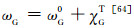
式中:ωG0为温度T外延至0K时G峰的拉曼位移,χGT为温度系数,单、双层石墨烯的温度系数分别为-0.016cm-1/℃和-0.015cm-1/℃。温度系数的确定,在测试过程中可仅通过石墨烯拉曼G峰的位置就可以检测测量环境温度的变化。与此同时,随着温度的上升,G峰和2D峰的半峰宽随之变大[65]。外界温度对拉曼光谱特征峰的影响由电子-声子的耦合作用、石墨烯的负热膨胀和声子-声子的非谐作用三个方面引起[66]。
3.3 激光能量对拉曼光谱的影响值得注意的是,激光光源的能量也会影响到D′峰和2D峰的峰值[67-68]。从图 12中可以看出[69],随着激光光源的能量的升高,石墨烯的D′峰向低频方向位移,2D峰向高频方向位移,与激光光源的能量之间具有高度的线性关系。乱层石墨(turbostratic graphite)的D′峰和2D峰的峰值随激光能量的变化关系与石墨烯相比存在一些微小差异。具体来说,随着激光能量的增大,单层石墨烯的2D峰峰值以88cm-1/eV的斜率增大,而乱层石墨的2D峰峰值以95cm-1/eV的斜率增大。石墨烯和石墨的D′峰峰值随激光能量的变化相较于2D峰没有那么明显,石墨烯的D′峰峰值随着激光能量的增大会以-18cm-1/eV的斜率减小,而乱层石墨的D′峰峰值以-31cm-1/eV的斜率减小[70]。在相关研究中也发现,随着激光能量的增大,石墨烯的D峰以50cm-1/eV的斜率增大[71]。激光光源的能量对拉曼特征峰峰值的影响主要由以下各个方面引起,激光诱导电子-空穴对的激发、电子-声子散射过程中的动量交换、缺陷散射和电子-空穴的复合[30]。

在石墨烯的拉曼测试中,激光功率的选择也至关重要,通常使用的功率在0.04~4mW范围内。图 13中显示了拉曼G峰峰值随激光功率的变化关系[72],可以看出,随激光功率的增加,G峰峰值以-1.226cm-1/mW的斜率降低。在这个功率范围内只会影响拉曼特征峰的峰值、峰型与强度,若功率过高,则会导致谱图的改变,或因激光的局部热效应使样品损坏甚至燃烧;若功率过低,则会导致拉曼光谱仪的信噪比过低[73]。
4 结束语
总的来说,近年来拉曼光谱在表征石墨烯方面的发展取得了巨大的突破。通过对石墨烯拉曼特征峰峰型、峰值和相对强度的变化的分析理解,可以快速准确地确定石墨烯的层数、堆垛顺序、缺陷密度和边缘手性。同时温度、基底、激光能量和激光光源等外界条件也会对拉曼光谱产生的影响。石墨烯作为未来高科技材料领域的主力军,人们对它的研究还在如火如荼地进行中。拉曼光谱作为一种灵敏便捷的表征方法,它在石墨烯的研究道路中起着十分重要的作用。它不仅可以被用来研究材料的电子结构和振动特性,还可以用来研究材料的能带结构和电子-声子相互作用,相信通过众多学者坚持不懈的研究,人们可以通过它更加深入地了解石墨烯。
| [1] | WALLACE P R. The band theory of graphite[J]. Physical Review, 1947, 71 (9): 622–634. DOI: 10.1103/PhysRev.71.622 |
| [2] | MCCLURE J W. Diamagnetism of graphite[J]. Physical Review, 1956, 104 (3): 666–671. DOI: 10.1103/PhysRev.104.666 |
| [3] | NOVOSELOV K S, GEIM A K, MOROZOV S V, et al. Electric field effect in atomically thin carbon films[J]. Science, 2004, 306 (5696): 666–669. DOI: 10.1126/science.1102896 |
| [4] | MEYER J C, GEIM A K, KATSNELSON M I, et al. The structure of suspended graphene sheets[J]. Nature, 2007, 446 (7131): 60–63. DOI: 10.1038/nature05545 |
| [5] | GEIM A K, NOVOSELOV K S. The rise of graphene[J]. Nature Materials, 2007, 6 (3): 183–191. DOI: 10.1038/nmat1849 |
| [6] | SHIN D, BAE S K, YAN C, et al. Synthesis and applications of graphene electrodes[J]. Carbon Letters, 2012, 13 (1): 1–16. DOI: 10.5714/CL.2012.13.1.001 |
| [7] | ZHANG Y B, TAN Y W, STORMER H L, et al. Experimental observation of quantum hall effect and Berry's phase in graphene[J]. Nature, 2005, 438 (7065): 1–7. |
| [8] | YANG H, HEO J, PARK S, et al. Graphene barrister, a triode device with a gate-controlled Schottky barrier[J]. Science, 2012, 336 (6085): 1140–1143. DOI: 10.1126/science.1220527 |
| [9] | LU J M, ZHANG H J, WU S, et al. Graphene magnetoresistance device in van der Pauw geometry[J]. Nano Letters, 2011, 11 (7): 2973–2977. DOI: 10.1021/nl201538m |
| [10] | ZHU Y, SUN Z Z, YAN Z, et al. Rational design of hybrid graphene films for high-performance transparent electrodes[J]. Acs Nano, 2011, 5 (8): 6472–6479. DOI: 10.1021/nn201696g |
| [11] | ARCO L G D, ZHANG Y, SCHLENKER C W, et al. Continuous, highly flexible, and transparent graphene films by chemical vapor deposition for organic photovoltaics[J]. Acs Nano, 2010, 4 (5): 2865–2873. DOI: 10.1021/nn901587x |
| [12] | WU C H, SHEN Q, DENG S X, et al. Preparation of novel three-dimensional NiO/ultrathin derived graphene hybrid for supercapacitor applications[J]. ACS Applied Materials&Interfaces, 2014, 6 (2): 1106–1112. |
| [13] | WU C H, SHEN Q, MI R, et al. Three-dimensional Co3O4/flocculent graphene hybrid on Ni foam for supercapacitor applications[J]. Journal of Materials Chemistry A, 2014, 2 (38): 15987–15994. DOI: 10.1039/C4TA03313B |
| [14] | FERRARI A C, MEYER J C, SCARDACI V, et al. Raman spectrum of graphene and graphene layers[J]. Physical Review Letters, 2006, 97 (18): 13831–13840. |
| [15] | KUZMANY H, PFEIFFER R, HULMAN M, et al. Raman spectroscopy of fullerenes and fullerene-nanotube composites[J]. Philosophical Transactions of the Royal Society A Mathematical Physical&Engineering Sciences, 2004, 362 (1824): 2375–2406. |
| [16] | DRESSELHAUS M S, DRESSELHAUS G, JORIO A, et al. Raman spectroscopy on isolated single wall carbon nanotubes[J]. Carbon, 2002, 40 (12): 2043–2061. DOI: 10.1016/S0008-6223(02)00066-0 |
| [17] | FERRARI A C, ROBERTSON J. Resonant Raman spectroscopy of disordered, amorphous, and diamondlike carbon[J]. Physical Review B Condensed Matter, 2001, 64 (7): 075414-1–075414-13. DOI: 10.1103/PhysRevB.64.075414 |
| [18] | MI R, LIU H, WANG H, et al. Effects of nitrogen-doped carbon nanotubes on the discharge performance of Li-air batteries[J]. Carbon, 2014, 67 (2): 744–752. |
| [19] | FERRARI A C, BASKO D M. Raman spectroscopy as a versatile tool for studying the properties of graphene[J]. Nature Nanotechnology, 2013, 8 (4): 235–246. DOI: 10.1038/nnano.2013.46 |
| [20] | MALARD L M, NILSSON J, ELIAS D C, et al. Probing the electronic structure of bilayer graphene by Raman scattering[J]. Physical Review B Condensed Matter, 2007, 76 (20): 1401-1–1401-4. |
| [21] | FERRARI A C, ROBERTSON J. Interpretation of Raman spectra of disordered and amorphous carbon[J]. Physical Review B Condensed Matter, 2000, 61 (20): 14095–14107. DOI: 10.1103/PhysRevB.61.14095 |
| [22] | DAS A, PISANA S, CHAKRABORTY B, et al. Monitoring dopants by Raman scattering in an electrochemically top-gated graphene transistor[J]. Nature Nanotechnology, 2008, 3 (4): 210–215. DOI: 10.1038/nnano.2008.67 |
| [23] | GRAF D, MOLITOR F, ENSSLIN K, et al. Spatially resolved raman spectroscopy of single-and few-layer graphene[J]. Nano Letters, 2007, 7 (2): 238–242. DOI: 10.1021/nl061702a |
| [24] | FERRARI A C. Raman spectroscopy of graphene and graphite:Disorder, electron-phonon coupling, doping and nonadiabatic effects[J]. Solid State Communications, 2007, 143 (1/2): 47–57. |
| [25] | YAN J, ZHANG Y B, KIM P, et al. Electric field effect tuning of electron-phonon coupling in graphene[J]. Physical Review Letters, 2007, 98 (16): 166802-1–166802-4. DOI: 10.1103/PhysRevLett.98.166802 |
| [26] | TUINSTRA F, KOENIG J L. Raman spectrum of graphite[J]. Journal of Chemical Physics, 1970, 53 (3): 1126–1130. DOI: 10.1063/1.1674108 |
| [27] | THOMSEN C, REICH S. Double resonant raman scattering in graphite[J]. Physical Review Letters, 2001, 85 (24): 5214–5217. |
| [28] | GARCIA S, MARIN A. Determination of LA and TO phonon dispersion relations of graphene near the Dirac point by double resonance Raman scattering[J]. Physical Review B, 2007, 76 (23): 233407-1–233407-4. DOI: 10.1103/PhysRevB.76.233407 |
| [29] | FERRARI A C, ROBERTSON J. Interpretation of Raman spectra of disordered and amorphous carbon[J]. Physical Review B, 2000, 61 (20): 14095–14107. DOI: 10.1103/PhysRevB.61.14095 |
| [30] | NEMANICH R J, SOLIN S A. First-and second-order Raman scattering from finite-size crystals of graphite[J]. Physical Review B, 1979, 20 (2): 392–401. DOI: 10.1103/PhysRevB.20.392 |
| [31] | GUPTA A, CHEN G, JOSHI P, et al. Raman scattering from high-frequency phonons in supported n-graphene layer films letters[J]. Nano Letters, 2006, 6 (12): 2667–2673. DOI: 10.1021/nl061420a |
| [32] | NI Z H, WANG Y Y, YU T, et al. Raman spectroscopy and imaging of grapheme[J]. Nano Research, 2008, 1 (4): 273–291. DOI: 10.1007/s12274-008-8036-1 |
| [33] | DAS A, CHAKRABORTY B, SOOD A K. Raman spectroscopy of graphene on different substrates and influence of defects[J]. Bulletin of Materials Science, 2007, 31 (3): 579–584. |
| [34] | PONCHARAL P, AYARI A, MICHEL T, et al. Raman spectra of misoriented bilayer graphene[J]. Physical Review B Condensed Matter, 2008, 78 (11): 113407-1–113407-8. DOI: 10.1103/PhysRevB.78.113407 |
| [35] | LOPES D S J M B, PERES N M R, CASTRO NETO A H. Graphene bilayer with a twist:electronic structure[J]. Physical Review Letters, 2008, 99 (25): 256802-1–256802-4. |
| [36] | MAK K F, SHAN J, HEINZ T F. Electronic structure of few-layer graphene:experimental demonstration of strong dependence on stacking sequence[J]. Physical Review Letters, 2010, 104 (17): 39–87. |
| [37] | NGUYEN T A, LEE J U, YOON D, et al. Excitation energy dependent Raman signatures of ABA-and ABC-stacked few-layer graphene[J]. Scientific Reports, 2014, 4 (7): 4630-1–4630-5. |
| [38] | LUI C H, LI Z, MAK K F, et al. Observation of an electrically tunable band gap in trilayer graphene[J]. Nature Physics, 2011, 7 (12): 944–947. DOI: 10.1038/nphys2102 |
| [39] | KIM M, CHOI S M, YOON H A, et al. Photocurrent generation at ABA/ABC lateral junction in tri-layer graphene photodetector[J]. Carbon, 2016, 96 : 454–458. DOI: 10.1016/j.carbon.2015.09.095 |
| [40] | LUI C H, LI Z, CHEN Z, et al. Imaging stacking order in few-layer graphene[J]. Nano Letters, 2010, 11 (1): 164–169. |
| [41] | CONG C X, YU T, SATO K, et al. Raman characterization of ABA-and ABC-stacked trilayer grapheme[J]. Acs Nano, 2011, 5 (11): 8760–8768. DOI: 10.1021/nn203472f |
| [42] | YAN J A, RUAN W Y, CHOU M Y. Phonon dispersions and vibrational properties of monolayer, bilayer, and trilayer graphene:density-functional perturbation theory[J]. Physical Review B Condensed Matter, 2009, 77 (12): 125401-1–125401-8. |
| [43] |
吴娟霞, 徐华, 张锦. 拉曼光谱在石墨烯结构表征中的应用[J].
化学学报, 2014, 72 (3): 301–318.
WU J X, XU H, ZHANG J. Raman spectroscopy of graphene[J]. Acta Chimca Sinica, 2014, 72 (3): 301–318. |
| [44] | YOU Y M, NI Z H, YU T, et al. Edge chirality determination of graphene by Raman spectroscopy[J]. Applied Physics Letters, 2008, 93 (16): 163112-1–1613112-3. DOI: 10.1063/1.3005599 |
| [45] | ZHANG X, LI Q Q, HAN W P, et al. Raman identification of edge alignment of bilayer graphene down to the nanometer scale[J]. Nanoscale, 2014, 6 (13): 7519–7525. DOI: 10.1039/C4NR00499J |
| [46] | BEGLIARBEKOV M, SUL O, KALLIAKOS S, et al. Determination of edge purity in bilayer graphene using micro-Raman spectroscopy[J]. Applied Physics Letters, 2010, 97 (3): 031908-1–031908-3. DOI: 10.1063/1.3464972 |
| [47] | CONG C X, YU T, WANG H M. Raman study on the g mode of graphene for determination of edge orientation[J]. Acs Nano, 2010, 4 (6): 3175–3180. DOI: 10.1021/nn100705n |
| [48] | ZHANG C H, FU L, LIU N, et al. Synthesis of nitrogen-doped graphene using embedded carbon and nitrogen sources[J]. Advanced Materials, 2011, 23 (8): 1020–1024. DOI: 10.1002/adma.v23.8 |
| [49] | HU G X. Raman spectroscopic characterization of graphene[J]. Applied Spectroscopy Reviews, 2010, 45 (1): 369–407. |
| [50] | PANCHAKARLA L S, SUBRAHMANYAM K S, SAHA S K, et al. Synthesis, structure and properties of boron and nitrogen doped graphene[J]. Advanced Materials, 2009, 21 (46): 4726–4730. |
| [51] | LIU L, RYU S, TOMASIK M R, et al. Graphene oxidation:Thickness-dependent etching and strong chemical doping[J]. Nano Letters, 2008, 8 (7): 1965–1970. DOI: 10.1021/nl0808684 |
| [52] | CANCADO L G, TAKAI K, ENOKI T, et al. General equation for the determination of the crystallite size La of nanographite by Raman spectroscopy[J]. Applied Physics Letters, 2006, 88 (16): 163106-1–163106-3. DOI: 10.1063/1.2196057 |
| [53] | WANG Y Y, NI Z H, YU T, et al. Raman studies of monolayer graphene:the substrate effect[J]. Journal of Physical Chemistry C, 2008, 112 (29): 10637–10640. DOI: 10.1021/jp8008404 |
| [54] | CASIRAGHI C, PISANA S, NOVOSELOV K S, et al. Raman fingerprint of charged impurities in graphene[J]. Applied Physics Letters, 2007, 91 (23): 233108-1–233108-3. DOI: 10.1063/1.2818692 |
| [55] | CALIZO I, BAO W Z, MIAO F, et al. Graphene-on-sapphire and graphene-on-glass:Raman spectroscopy study[J]. Physics, 2007, 91 (20): 201904-1–201904-9. |
| [56] | CALIZO I, TEWELDEBRHAN D, BAO W Z, et al. Spectroscopic Raman nanometrology of graphene and graphene multilayers on arbitrary substrates[J]. Journal of Physics Conference Series, 2008, 109 (1): 012008-1–012008-4. |
| [57] | OHTA T, BOSTWICK A, SEYLLER T, et al. Controlling the electronic structure of bilayer graphene[J]. Science, 2006, 313 (5789): 951–954. DOI: 10.1126/science.1130681 |
| [58] | VARCHON F, FENG R, HASS J, et al. Electronic structure of epitaxial graphene layers on SiC:effect of the substrate[J]. Physical Review Letters, 2007, 99 (12): 126805-1–126905-5. DOI: 10.1103/PhysRevLett.99.126805 |
| [59] | CELEBI C, YANIK C, DEMIRKOL A G, et al. The effect of a SiC cap on the growth of epitaxial graphene on SiC in ultra high vacuum[J]. Carbon, 2012, 50 (8): 3026–3031. DOI: 10.1016/j.carbon.2012.02.088 |
| [60] | NI Z H, CHEN W, FAN X F, et al. Raman spectroscopy of epitaxial graphene on a SiC substrate[J]. Physical Review B, 2008, 77 (11): 115416-1–115416-20. DOI: 10.1103/PhysRevB.77.115416 |
| [61] | ABDULA D, OZEL T, KANG K, et al. Environment-induced effects on the temperature dependence of Raman spectra of single-layer graphene[J]. Journal of Physical Chemistry C, 2008, 112 (51): 20131–20134. DOI: 10.1021/jp809501e |
| [62] | CALIZO I, MIAO F, BAO W, et al. Variable temperature Raman microscopy as a nanometrology tool for graphene layers and graphene-based devices[J]. Applied Physics Letters, 2007, 91 (7): 071913-1–071913-3. DOI: 10.1063/1.2771379 |
| [63] | CALIZO I, BALANDIN A A, BAO W Z, et al. Temperature dependence of the Raman spectra of graphene and graphene multilayers[J]. Nano Letters, 2007, 7 (9): 2645–2649. DOI: 10.1021/nl071033g |
| [64] | CALIZO I, LAU C N. Raman nanometrology of graphene on arbitrary substrates and at variable temperature[J]. Proceedings of SPIE-The International Society for Optical Engineering, 2008, 7037 : 70371B-1–70371B-8. |
| [65] | ZHOU H Q, QIU C Y, YU F, et al. Raman scattering of monolayer graphene:the temperature and oxygen doping effects[J]. Journal of Physics D Applied Physics, 2011, 44 (18): 237–251. |
| [66] | LATE D J, MAITRA U, PANCHAKARLA L S, et al. Temperature effects on the Raman spectra of graphenes:dependence on the number of layers and doping[J]. Journal of Physics Condensed Matter, 2011, 23 (5): 55303–55307. DOI: 10.1088/0953-8984/23/5/055303 |
| [67] | CANCADO L G, JORIO A, FERREIRA E H M, et al. Quantifying defects in graphene via Raman spectroscopy at different excitation energies[J]. Nano Letters, 2011, 11 (8): 3190–3196. DOI: 10.1021/nl201432g |
| [68] | PARK J S, REINA A, SAITO R, et al. G'band Raman spectra of single, double and triple layer grapheme[J]. Carbon, 2009, 47 (5): 1303–1310. DOI: 10.1016/j.carbon.2009.01.009 |
| [69] | MAFRA D L, SAMSONIDZE G G, MALARD L M, et al. Deterination of LA and TO phonon dispersion relations of grapehene near the Dirac point by double resonance Raman scattering[J]. Physical Review B, 2007, 76 (23): 233407-1–233407-4. DOI: 10.1103/PhysRevB.76.233407 |
| [70] | MALARD L M, PIMENTA M A, DRESSELHAUS G, et al. Raman spectroscopy in graphene[J]. Physics Reports, 2009, 473 (5): 51–87. |
| [71] | POCSIK I, HUNDHAUSEN M, KOOS M, et al. Origin of the D peak in the Raman spectrum of microcrystalline graphite[J]. Journal of Non-Crystalline Solids, 1998, 227/230 (1): 1083–1086. |
| [72] | CALIZO I, GHOSH S, BAO W Z, et al. Raman nanometrology of graphene:temperature and substrate effects[J]. Solid State Communications, 2009, 149 (27/28): 1132–1135. |
| [73] |
杰米.
石墨烯:基础及新兴应用[M]. 北京: 科学出版社, 2014: 199.
WARNER J H. Graphene:fundamentals and emergent application[M]. Beijing: Science Press, 2014: 199. |