 2013, Vol. 1
The article information
- H. Xu, T. Suni, V. Vuorinen, J. Li, H. Heikkinen, P. Monnoyer, M. Paulasto-Kröckel
- Wafer-level SLID bonding for MEMS encapsulation
- Advances in Manufacturing, 2013, 1(3): 226–235
- http://dx.doi.org/10.1007/s40436-013-0035-0
-
Article history
- Received: 2013-07-26
- Accepted: 2013-08-19
- Published online: 2013-09-06


2. VTT Technical Research Centre of Finland, Espoo, Finland
Micro electronic mechanical system (MEMS) devices often require a sealed environment for optimal performance. In a large variety of applications,the functional structures in MEMS devices have to be capped hermetically and protected from such things as moisture,particles, gases,and physical loads. For many MEMS devices,there is a requirement for low operating pressure inside the package,which originates from the need to minimize the air film damping of the vibrating structures. In these packages,leaking may induce losses such as air damping, which will compromise the device's performance or even make the device stop functioning altogether. Thus the lifetime of the MEMS devices is highly dependent on the integrity of the bonds. The encapsulation methods that are traditionally used include anodic,glass frit,and metal bonding. Metal bonding can also be divided into the following sub-categories: eutectic bonding,solder bonding, and solid-liquid interdiffusion (SLID) (or transient liquidphase (TLP)) bonding [1, 2, 3].
SLID bonding designed for semiconductor joining was described as "a process whereby high-temperature phases are formed by diffusion in the presence of liquid",and also "a technique which utilizes these phenomena in producing high-temperature-stable bonds which have been fabricated at low temperatures" by Bernstein [4]. Ag-In,Au-In and Cu-In metal systems had been discussed in his study. And later,researchers figured out how to exploit more metal systems for SLID bonding,including Ag-Sn [5],Au-Sn [6, 7, 8, 9, 10],Cu-Sn [11, 12, 13] and Ni-Sn [14, 15],for semiconductor packaging. Some ternary metal systems have also been developed,such as Cu/Ni/Sn [16, 17]. This SLID bonding method,which is already commonly utilized to assemble power electronic components [18],is now also becoming more and more popular in other fields as well,such as 3D packaging. Agarwal et al. [13] utilized Cu-Sn SLID for die stacking in 3D integration. Similarly,Liu et al. [19] performed wafer-level Cu-Sn SLID interconnects in a vacuum, which is promising for 3D assembly and packaging. For their part,Klumpp et al. [20, 21] proposed a waferlevel, 3D integration approach called inter chip via-solidliquid interdiffusion (ICV-SLID),which is a new chip-towafer stacking technology that can be combined with SLID for copper and tin and the inter chip via (ICV) process to form multiple device stacks. In some cases,the SLID can even be used in other applications besides the semiconductor industry,such as superalloy bonding [22] and the joining of structural intermetallic compounds (IMCs) [23].
Most of the SLID bonding applications designed for the electrical interconnections and the die attachments in the 3D packaging can directly be used for the MEMS packaging. In addition,the application of the SLID bonding technology in hermetic sealing for vacuum is becoming more and more attractive and important in terms of MEMS packaging for the industry in addition to the traditional AuSn solder and eutectic Au-Si bonding,especially considering the fact that the melting temperature of the sealing metals is much lower than the re-melting temperature of the formed IMCs. In addition,metals have a higher density than glass materials,and,as such,a lower gas permeability, thus making metals very suitable for hermetic sealing. The flexibility of utilizing many different metal combinations can meet the various requirements for manufacturability, functionality,and reliability,especially when considering that the low melting point metal combination (< 400 °C) can lower the bonding process temperature,which can lead to lower thermo-mechanical stresses. In addition,the footprint of the devices can be minimized by using narrow metallic seal rings. Therefore,the metal encapsulation may also significantly increase the lifetime of MEMS devices in high temperature applications [24]. Welch et al. [25, 26] tested the Ni-Sn and the Au-In metal combinations to MEMS wafer level vacuum packaging. They sealed the Pirani gauge in the vacuum with the bond rings,and focused on the pressure change of the sealed space in a long service time. This SLID bonding was also combined with wafer-level solder transfer technique by Welch et al. [27] to transfer a metal MEMS cap and bond it to a device wafer simultaneously. Vivek et al. [28] proposes two prospective candidates,Al-Ge and Pt-In,for hermetic sealing of MEMS sensor for rugged environment applications. They made a conclusion that Al-Ge eutectic is a more prospective candidate for harsh environments due to its immunity to thermal degradation. Marauska et al. [29] present the low temperature and high quality SLID bonds of Au/Sn and Cu/Sn electroplated material systems designed for MEMS wafer-level hermetic vacuum sealing.
However,the design of the metal layers and the important factors concerning of both the microstructure and the bond quality are not quite available. Thus,in this work,the design of two metal bond combinations of Au-Sn and Cu-Sn are studied. The principle for the layer's structure design is discussed. The microstructure of the rings after bonding is also studied. We chose to use the shear test to evaluate the mechanical properties of the bond rings. Failure analysis will reveal the effect of the bond ring design on mechanical properties and the reliability of the bond rings. 2 Principle of SLID bonding
SLID bonding uses the low melting temperature of the filler alloy and forms a high-melting and non-ductile joint. The difference between the low processing temperature and the final high-melting temperature is one of the most interesting benefits of SLID bonding,which allows for sequential processing at the same process temperature. With the SLID process,at least one low-melting metal and one high-melting metal are involved,which can form IMC phases. The metal thickness has to be in the range of a few microns to finish the process within a reasonable amount of time. Generally,SLID bonding consists of four stages: melting,dissolution,isothermal solidification,and homogenization. Once the bonding temperature is above the eutectic point for the metal system in question,a liquid phase appears. Then,the low-melting-point metal begins to react with the base metals and is gradually transformed into IMCs,which have a higher melting point than that of the interlayer. Depending on the process parameters (namely temperature and time),the joint is either formed by way of solidification from a specified nominal composition or it undergoes isothermal solidification. The former is typical in Au-Sn-based solutions and the latter in Cu-Sn-based solutions. A valuable review of the theory of the SLID bonding process has been provided by Zhou et al. [30].
Figure 1 schematically shows the formation of the hermetic bond using the Au-Sn system. The phase diagram used here is from a study by Okamoto [31]. After the initial contact of the metallizations has been obtained and temperature has risen above the eutectic temperature of 215 °C for the system,liquid forms at the interface. Typically,the process temperature is well above the melting point of Sn and the dissolution of the Au is rapid (in the order of μm/s), since the solubility of Au in liquid Sn is high. In principle, the Sn liquid is first consumed by the formation of AuSn, which is then re-melted when more gold is diffused from the reaction layer. Basically,a concentration profile in liquid should then exist,which should be in equilibrium with both the AuSn and hcp phase. However,since these reactions occur quite rapidly,the solid state diffusion mechanisms do not have time to contribute to the process. Therefore,the analysis can be simplified by assuming that the dissolving Au is mixed into the Sn liquid,thereby forming a certain average nominal composition. This composition is defined by the process temperature,the time,as well as the thickness of the Sn layer. Take the nominal Au atomic percentage of 76 % as an example,as shown in Fig. 1. The nominal composition is located in the region of "L + hcp". Within the structure,the liquid Au- Sn phase will come into equilibrium with some amount of the primary hcp phase. When the cooling starts,the grains of the primary hcp phase grow upwards,and liquid phase remains in equilibrium with the hcp phase until a eutectic temperature of 278 °C is reached. Once the eutectic temperature has been reached,the rest of the liquid is consumed by the simultaneous formation of the AuSn and hcp phase. As the cooling continues,the relative amount of the hcp phase decreases while the AuSn phase increases until the hcp phase becomes unstable at 190 °C and is transformed into Au5Sn. Hence,the stable structure at room temperature consists of the primary Au5Sn phase and a two-phase mixture eutectic structure of the AuSn and the Au5Sn. It must be emphasized that thermodynamic equilibrium is assumed throughout our analysis and that, for example,nucleation as well as the undercooling effects are neglected in this paper.
 |
| Fig. 1 Schematic presentation of the formation of the Au-Sn SLID joint (with a higher Sn ratio): the yellow and gray dots in phase diagram [31] represent the original Au and Sn,the red dot is the average composition of the liquid before cooling,and the dark blue,light blue and green dots represent the composition of the Au5Sn,hcp and AuSn phases,respectively |
Since the nominal Au atomic percentage is up to 84 %, as shown in Fig. 2,the composition is located in the region of the "hcp" phase. If there is still a base Au left,the hcp grain initials on the interface and then grows gradually into the liquid until it consumes all of the tin. The structure consists of a residual gold and hcp phase. When cooling to 190 °C,the hcp phase becomes unstable and is transformed into Au5Sn. Thus,the stable structure at room temperature mainly consists of the Au5Sn phase.
 |
| Fig. 2 Schematic presentation of the formation of the Au-Sn SLID joint (with a lower Sn ratio): the yellow and gray dots in phase diagram [31] represent the original Au and Sn; the red dot is the average composition of the liquid before cooling; and the dark blue and light blue dots represent the composition of Au5Sn and hcp,respectively |
Figure 3 schematically shows the formation of the hermetic bond utilizing the Cu-Sn system. The phase diagram comes from a study by Fu¨rtauer et al. [32]. After the initial contact of the metallizations,and after the temperature has increased above the eutectic temperature (222 °C of the Cu-Sn system),the formation of liquid occurs at the interface between Cu and Sn. In principle,the liquid Sn is first consumed by the formation of Cu6Sn5,which is then transferred into Cu3Sn in a solid state when more copper is diffused from the reaction layer,as shown in Fig. 3. Hence, the stable structure at room temperature consists of a residual Cu and Cu3Sn phase,which is thermally stable up to 640 °C [33, 34, 35].
 |
| Fig. 3 Schematic presentation of the formation of the Cu-Sn SLID joint: the yellow and gray dots in phase diagram [32] represent the original Au and Sn,while the red dot and blue dot represent the composition of Cu3Sn and Cu6Sn5,respectively |
For the sample preparation of both the Au-Sn bonding and the Cu-Sn bonding,standard double side polished (DSP) 150 mm silicon wafers were used as handle wafers and single side polished (SSP) wafers as cap wafers. The back side alignment marks were fabricated on the handle wafer before bonding for alignment. A thin titanium tungsten layer was used as an adhesion layer between the silicon and the seed layer. Gold or copper seed layers were sputtered to the front side of both the handle and the cap wafers. A copper seed layer was used for making CuSn seal rings and a gold seed layer for making AuSn seal rings. During the lithography process,a thick photoresist was coated on the surface and removed from the seal ring areas. The seal rings were electroplated to the resist openings using the Everplate Cu 200 chemicals from Atotech for the copper bath,Neutronex 309 from Enthone for the Au bath and Solderon BP from Rohm & Haas for the Sn bath. The target thickness for the gold and copper electroplating in both the handle wafer and cap wafer was 4 μm and 6 μm,respectively. Three different bonding schemes were tested in this study,as shown in Fig. 4a: (i) The handle wafer has Sn and Au layers,whereas the cap wafer has only an Au layer (for short,written as AuSn-Au); (ii) the handle wafer and the cap wafer have the same Sn and Au layers structure (for short,written as AuSn-SnAu); and (iii) the handle wafer and the cap wafer have the same Sn and Cu layers structure (for short,written as CuSn-SnCu). The total thickness of the Sn is 2 μm for AuSn-Au bonding and 4 μm for AuSn- SnAu and CuSn-SnCu bonding. The seal ring thickness and thickness uniformity were measured after resist removal using a profilometer. The dimension of the ring is 1,576 μm × 783 μm,with the width being 60 μm. The seal ring fabrication process steps are shown in Fig. 4b.
 |
| Fig. 4 Schematics of the seal ring structure and production process flow |
After the seal ring structures were ready,the wafers were aligned and placed on a bonding chuck using EVG620 bond aligner. Then,the bonding chuck was transferred to the bonding chamber of the EVG501 wafer bonder. The wafer pair was kept in a vacuum (0.1 Pa) for 30 min,after which the wafers were brought into contact; a pressing force of 3.5 kN was applied and the chamber heating was switched on. Three different bonding parameters were used for the three bonding schemes: (i) For AuSn-Au,the bonding chamber was heated to 350 °C and kept at this temperature for 30 min; (ii) for AuSn-SnAu, the bonding temperature was 320 °C and lasted for 60 min; and (iii) for CuSn-SnCu,the bonding temperature was 300 °C and lasted for 30 min. The whole bonding process took 3.5-6.0 h,including both the heating and cooling process. All the wafers were diced into small chips with a dimension of 5 mm × 5 mm,and each chip included 12 seal rings arrayed in 2 columns. The bonding quality of the seal rings was analyzed using cross-sectional scanning electron microscopy (SEM).
The MTS 858 table test system was used for conducting a shear test of the chips from the diced bond wafers in order to evaluate the bonding quality as well as to find out the mechanical failure mechanism of the bond rings. Figure 5a shows the designed holder for the specimens and the general experimental setup. The shear direction is along the long side of the seal rings. The shear speed used in this study was 0.01 mm/s. Finite element analysis was employed to study the non-uniform stress distribution in the seal rings during the shear test. The simulation was carried out using a finite element package: the ABAQUS v. 6.12-3. As shown in Fig. 5b,only half of the sample was modeled due to symmetry and the right-sided surface was the symmetry surface. In terms of boundary conditions,the bottom of the lower silicon chip was fixed,while displacement loading was applied to the top silicon chip.
 |
| Fig. 5 Shear test setup and simulation model |
Two different Au-Sn compositions are compared to demonstrate the design of the seal ring structures,which was achieved using AuSn-Au and AuSn-SnAu bonding,as described above. 4.1.1 AuSn-Au bonding
In AuSn-Au bonding,the Sn layer only exists on the handle wafer side. During bonding,the Sn layer will melt and react with the Au layers along both sides of the wafer. The thickness of Sn is 2 μm and the total thickness of the two Au layer on both the substrate side and the cap side is 8 μm. The Sn mole percentage is approximately 13.5 % in the seal ring,if complete mixing is assumed. Based on the discussion in Sect. 2,the microstructure of the ring should include Au5Sn and residual Au after remaining at a temperature of 350 °C for 30 min. In the final rings,it is quite common to find out that the residual Au existed only in the cap wafer side,as shown in Fig. 6a.
 |
| Fig. 6 Microstructure of the Au-Sn bonding at different ratios |
In AuSn-SnAu bonding,both the handle wafer and the cap wafer had the same AuSn layer structure: 2 μm for Sn and 4 μm for Au. The average Sn mole percentage in the seal ring is now 23.8 %. According to the Au-Sn binary phase diagram in Sect. 2,the excessive amount of Sn will consume all of the Au layer in the ring after bonding at 320 °C for 60 min and the final microstructure should consist of a primary Au5Sn and Au5Sn/AuSn eutectic structure. As shown in Fig. 6b,the real cross-sectional SEM image shows the main part of the ring is primary Au5Sn,and the eutectic structure can be found at the edge of ring. The interfacial microstructure can be observed after peeling off the cap wafer and the Ti(W) adhesion layer,as shown in Fig. 6c. The Au5Sn and AuSn eutectic structure can also be found at the interface close to the Ti(W) adhesion layer. 4.2 Mechanical properties of Au-Sn seal rings
We conducted shear tests to evaluate the bonding quality as well as the effects of defects in the seal rings. Normally,the shear loading is assumed to be uniformly distributed over all the seal rings,and then this uniform assumption is often used to calculate the shear strength of the bonding. However, in reality the stress-strain distributions in the seal rings are extremely heterogeneous. Figure 7 shows the first principal stress and strain distributions of the seal rings at the time point just before cracking. It is obvious that the stress concentration was located at the ring's short edges, close to the outer boundaries. This finding tells us that at the initial stage of the shear test,the short edges were holding most of the shear loading until they failed due to cracking. The crack propagation path in one ring should start from the short side close to the boundary and proceed to the other short side close to the chip center. Furthermore, among the three short edges shown in the strain distribution image,the leftmost one experienced the highest level of stress because the seal ring was located close to the free edge of the sample. The seal ring located in the top left corner is supposed to fail first,following by the rest of the seal rings.
 |
| Fig. 7 First principal stress and strain distributions of the seal rings during the shear test |
In the real tests,the average maximum shear force for the void samples involved in AuSn-Au bonding was 365 N,with a standard deviation of 30 N. In comparison, the average maximum shear force is only 183 N (with a standard deviation of 23 N) for AuSn-SnAu bonding, which is only half of the value of the AuSn-Au bond rings. There are two different failure mechanisms found for AuSn-Au bonding,and AuSn-SnAu bonding occurs separately. 4.2.1 AuSn-Au bonding
We observed large voids in the middle part of the ring,as shown in Fig. 8a. These voids can affect the crack propagation path during the shear test. The fracture surface of the seal ring from the cap wafer and handle wafer can be observed in Fig. 8b and c. Only a small part of the bond remains on the handle wafer side. The major part of the bond is left on the cap wafer side. The location of the voids in the ring can easily be found in the middle of the fractured ring,as shown in Fig. 8b. Figure 8d shows a cross section of the two departed pieces. Based on the higher stress level at these locations during the simulation,we can assume that the crack initiates at the interface of the Au5Sn and Ti(W) layer along the outer short side of the rings. Then,when the crack tip reaches the void location,the crack will propagate into the voids due to the stress concentration generated by the voids. Eventually,the crack will emerge from the void and go back to the interface along the inner short side of the rings.
 |
| Fig. 8 AuSn-Au microstructure after bonding and the defect for the huge void in the middle of the ring |
The voids come from the uneven Sn layer on the Au metallization,especially when the Sn plating chemistry is not in optimal condition. At the edges of these rings,there will be much thicker Sn than on the other parts of the ring, as shown in Fig. 9. The high edge of the rings may stop the contact of the middle part; in such instances,the voids in the middle of the ring will form during cooling. This means that the thickness uniformity of the layers in the ring is extremely important concerning the mechanical reliability of the rings.
 |
| Fig. 9 Uneven Sn layer in the plating rings before bonding |
We used flat and uniform Au and Sn layers for AuSn-SnAu bonding,rarely finding the voids. The failure analysis shows that the crack mainly propagates along the interface between the Au-Sn seal ring and the Ti(W) adhesion layer, as shown in Fig. 10. It is highly probable that the direct contact of the AuSn eutectic structure with the Ti(W) layer is the main reason that the average maximum shear force is much lower than the AuSn-Au force.
 |
| Fig. 10 Two sides of the AuSn-SnAu bond ring shear fracture surface |
The results in Sect. 4.2 indicate that the interface bond between the Au5Sn/AuSn eutectic structure and the Ti(W) layer is weaker than the Au5Sn and Ti(W) interface. And it should be noticed that in AuSn-Au bonding both of the two different interfaces,the Au-Ti(W) interface and the Au5Sn-Ti(W) interface,existed in the same ring,but it was rare to find the fracture at the Au and Ti(W) interface. Likewise,all of the observed failures were at the Au5Sn and Ti(W) interface. It means that the bonding at the Au- Ti(W) interface seems to be much stronger than at the Au5Sn-Ti(W) interface. Anyhow,the results show that the most reliable interface,which should also be the target interface,is the Au-Ti(W) interface,especially when designing the metallization thicknesses with respect to bonding process parameters. On the one hand,in order to meet the reliability requirement,the direct contact of the Au5Sn-AuSn eutectic structure with the Ti(W) adhesion layer is not acceptable. On the other hand,the thickness of the Sn layer decides the amount of liquid needed during bonding,which definitely has a limitation that needs to be reduced. Hence,to solve this problem,the choice can either be to increase the amount of Au,which will clearly increase costs,or to utilize a diffusion barrier. For example, Ni seems to be a good choice for barrier material,since the reaction between Ni and AuSn IMCs is rather slow. 4.4 Cu-Sn materials system
In CuSn-SnCu bonding,Sn layers exist on both the cap and handle wafers. The total thickness of Sn is 4 μm,whereas the thickness of the two Cu layers from both the substrate and the cap wafers is 12 μm. The average Sn mole percentage is approximately 12.7 % in the seal ring,if complete mixing is assumed. After bonding at 300 °C for 30 min,the targeted microstructure of the ring should mainly include Cu3Sn and residual Cu,as shown in Fig. 11a. A small amount of Cu6Sn5 will still be unconsumed at the corner of the rings in most cases,as shown in Fig. 11b. Since Cu6Sn5 has a lower elastic module [36] and a smaller fracture toughness than Cu3Sn [37, 38],it is more prone to fracture under the mechanical load. Such Cu6Sn5 might be the initial nucleation site for cracks,and then the cracks could propagate along the interface between Cu6Sn5 and Cu3Sn and finally go inside the bonded region and proceed into the Cu3Sn layer.
 |
| Fig. 11 Microstructure of CuSn-SnCu bonding |
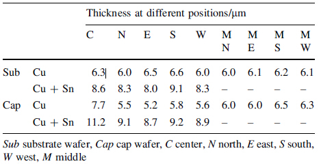
Here it has to be pointed out that the uniformity of the Cu layer thickness,which is similar to the Sn layer thickness in Au-Sn bonding,also plays an important role in the mechanical property of the bond rings. We measured the thickness of pure Cu after Cu plating and the thickness of both the Cu and Sn layers after Sn plating separately at 9 positions on the wafer,and the corresponding values of each point can be found in Table 1. It can easily be seen that the rings at the center of both the handle wafer and the cap wafer are generally thicker than the ones along the edge of these wafers. The thickness distribution at the middle part of the wafer is more uniform. This non-uniformity of thickness can cause a difference in bonding quality all around the wafer: More squeeze-out (containing Cu and Sn) at the center parts of the wafers and more non-bonded regions in the rings along the outer parts of the wafers,as shown separately in Fig. 12a and b. In comparison,the middle part of the wafer has a better quality,as shown in Fig. 10,since the middle part on the wafer has a more uniform thickness after plating. We tested the shear strength of the chip at different locations. Figure 12c shows that the trend of maximum shear force is drawn with distance from the wafer's center. The rings at both the center and the edge of the wafer have lower shear force than the ones in the middle part. The maximum force differences can reach more than 150 N,over one quarter of the average shear force.
 |
 |
| Fig. 12 Effect of Cu layer thickness on the bond's quality and shear force |
The design principles for Au-Sn and Cu-Sn SLID bonding are studied in this paper. A different ratio of the metals, especially the Au-Sn ratio,will result in a different microstructure in the rings. Metal systems,including AuSn-Au,AuSn-SnAu,and CuSn-SnCu,are chosen in this work to achieve real bonding for MEMS devices.
For AuSn-Au bonding,the as-bond ring consisted of Au5Sn and residual Au. The voids in the center of the rings are the main defects that can significantly change the crack propagation path. The cracks in the bond rings started at the Au5Sn and Ti(W) interface and then propagated into the defect of voids. For AuSn-SnAu bonding,the as-bond ring consisted of primary Au5Sn and the eutectic structure of Au5Sn and AuSn IMCs. The excessive Sn atoms that accumulated at the interface will reduce the shear strength of rings significantly. The comparison between AuSn-Au and AuSn-SnAu bonding shows that the Au-Ti(W) interface, which is stronger than the Au5Sn-Ti(W) interface and the AuSn/Au5Sn-Ti(W) interface,should be the target interface for bond structure design.
For CuSn-SnCu bonding,the ring mainly consisted of Cu3Sn and residual Cu. Only a small amount of Cu6Sn5 existed at the corner of the rings,which can initiate the cracks during shear testing. The non-uniformity of the Cu layer can induce large variations in the shear strengths around the wafer area.
Acknowledgments This work has been carried out as part of a Tekes Project: Real_metal (Grants Nos. 40009/12,40010/12). The authors would like to acknowledge the Finnish Funding Agency for Technology and Innovation (Tekes),Okmetic Oyj,and Murata Electronics for funding.| 1. | Suhir E, Lee YC, Wong CP (2007) Micro- and optoelectronic materials and structures: physics, mechanics, design, reliability, packaging. Springer, New York |
| 2. | Tummala RR, Swaminathan M (2008) Introduction to system-onpackage: miniaturization of the entire system. McGraw-Hill,NewYork |
| 3. | Hartzell AL, Silva MG, Shea HR (2010) MEMS reliability. Springer, Brookline |
| 4. | Bernstein L (1966) Semiconductor joining by the solid-liquidinterdiffusion (SLID) process: I. The systems Ag-In, Au-In, and Cu-In. J Electrochem Soc 113(12):1282-1288 |
| 5. | Li JF, Agyakwa PA, Johnson CM (2010) Kinetics of Ag3Sn growth in Ag-Sn-Ag system during transient liquid phase soldering process. Acta Mater 58(9):3429-3443 |
| 6. | Tollefsen TA, Larsson A, Løvvik OM et al (2012) Au-Sn SLID bonding-properties and possibilities. Metall Mater Trans B 43(2):397-405 |
| 7. | Matijasevic GS, Lee CC, Wang CY (1993) AuSn alloy phase diagram and properties related to its use as a bonding medium. Thin Solid Films 223(2):276-287 |
| 8. | Lee CL, Wang YW, Matijasevic G (1993) Advances in bonding technology for electronic packaging. J Electron Packag 115(2): 201-207 |
| 9. | Johnson WR, Wang CQ, Liu Y et al (2007) Power device packaging technologies for extreme environments. IEEE Trans Electron Packag Manuf 30(3):182-193 |
| 10. | Wang K, Aasmundtveit K, Jakobsen H (2008) Surface evolution and bonding properties of electroplated Au/Sn/Au. In: Electronics system-integration technology conference, Greenwich, 1-4 Sept 2008, pp 1131-1134 |
| 11. | Bartels F, Morris JW, Dalke G et al (1994) Intermetallic phase formation in thin solid-liquid diffusion couples. J Eletron Mater 23(8):787-790 |
| 12. | Bosco NS, Zok FW (2005) Strength of joints produced by transient liquid phase bonding in the Cu-Sn system. Acta Mater 53(7):2019-2027 |
| 13. | Agarwal R, Zhang W, Limaye P et al (2009) High density Cu-Sn TLP bonding for 3D integration. In: Electronic components and technology conference (ECTC 2009. 59th), San Diego, CA, 26-29 May 2009, pp 345-349 |
| 14. | Welch W, Chae J, Lee SH et al (2005) Transient liquid phase (TLP) bonding for microsystem packaging applications. The 13th international conference on solid-state sensors, actuators and microsystems. doi:10.1109/SENSOR.2005.1497331 |
| 15. | Esashi M (2008) Wafer level packaging of MEMS. J Micromech Microeng 18(7):073001 |
| 16. | Dimcic B, Messemaeker JD, Zhang W et al (2012) Phase formation in Cu/Ni/Sn thin film systems. In: Electronics system integration technologies conference (ESTC). doi:10.1109/ESTC. 2012.6542137 |
| 17. | Zhang W, Dimcic B, Limaye P et al (2011) Ni/Cu/Sn bumping scheme for fine-pitch micro-bump connections. In: Electronic components and technology (ECTC), Lake Buena Vista, FL, May 31-June 3 2011, pp 109-113 |
| 18. | Brem F, Liu C, Raik D (2012) Influence of Cu joining partner in transient liquid phase bonding. In: Electronics system integration technologies conference (ESTC). doi:10.1109/ ESTC.2012.6542135 |
| 19. | Liu H, Salomonsen G, Wang K et al (2011) Wafer-level Cu/Sn to Cu/Sn SLID-bonded interconnects with increased strength. IEEE Trans Comput Packag Manuf 1(9):1350-1358 |
| 20. | Klumpp A, Merkel R, Ramm P et al (2004) Vertical system integration by using inter-chip vias and solid-liquid interdiffusion bonding. Jpn J Appl Phys 43(7A):L829-L830 |
| 21. | Wieland R, Bonfert D, Klumpp A et al (2005) 3D integration of CMOS transistors with ICV-SLID technology. Microelectron Eng 82(3/4):529-533 |
| 22. | Pouranvari M, Ekrami A, Kokabi AH (2009) Effect of bonding temperature on microstructure development during TLP bonding of a nickel base superalloy. J Alloy Compd 469(1/2):270-275 |
| 23. | Gale WF (1999) Applying TLP bonding to the joining of structural intermetallic compounds. JOM 51(2):49-52 |
| 24. | Tollefsen TA, Taklo MMV, Aasmundtveit KE et al (2012) Reliable HT electronic packaging-optimization of a Au-Sn SLID joint. In: Electronics system integration technologies conference (ESTC). doi:10.1109/ESTC.2012.6542138 |
| 25. | Welch WC, Najafi K (2007) Nickel-tin transient liquid phase (TLP) wafer bonding for MEMS vacuum packaging. In: Solidstate sensors, actuators and microsystems conference. doi:10.1109/SENSOR.2007.4300385 |
| 26. | Welch WC, Najafi K (2008) Gold-indium transient liquid phase (TLP) wafer bonding for MEMS vacuum packaging. In: Micro electro mechanical systems (MEMS 2008), Tucson, AZ, 13-17 Jan 2008, pp 806-809 |
| 27. | Welch WC, Junseok C, Najafi K (2005) Transfer of metal MEMS packages using a wafer-level solder transfer technique. IEEE Trans Adv Packag |
| 28. | Vivek C, Ho BY, Gao S (2012) Development of metallic hermetic sealing for MEMS packaging for harsh environment applications. J Eletron Mater 41(8):2256-2266 |
| 29. | Marauska S, Claus M, Lisec T et al (2012) Low temperature transient liquid phase bonding of Au/Sn and Cu/Sn electroplated material systems for MEMS wafer-level packaging. Microsyst Technol 19(8):1119-1130 |
| 30. | Zhou Y, Gale WF, North TH (1995) Modelling of transient liquid phase bonding. Int Mater Rev 40(5):181-196 |
| 31. | Okamoto H (2007) Au-Sn (gold-tin). J Phase Equilib Diffus 28(5):490 |
| 32. | Fürtauer S, Li D, Cupid D et al (2013) The Cu-Sn phase diagram, part I: new experimental results. Intermetallics 34:142-147 |
| 33. | Lueck MR, Reed JD, Gregory CW et al (2012) High-density large-area-array interconnects formed by low-temperature Cu/Sn- Cu bonding for three-dimensional integrated circuits. IEEE Trans Electron Dev 59(7):1941-1947 |
| 34. | MacDonald WD, Eagar TW (1992) Transient liquid phase bonding. Annu Rev Mater Sci 22:23-46 |
| 35. | Bader S, Gust W, Hieber H (1995) Rapid formation of intermetallic compounds interdiffusion in the Cu-Sn and Ni-Sn systems. Acta Metall Mater 43(1):329-337 |
| 36. | Song JM, Shen YL, Su CW et al (2009) Strain rate dependence on nanoindentation responses of interfacial intermetallic compounds in electronic solder joints with Cu and Ag substrates. Mater Trans 50(5):1231-1234 |
| 37. | Balakrisnan B, Chum CC, Li M et al (2003) Fracture toughness of Cu-Sn intermetallic thin films. J Electron Mater 32(3):166-171 |
| 38. | Ghosh G (2004) Elastic properties, hardness, and indentation fracture toughness of intermetallics relevant to electronic packaging. J Mater Res 19(5):1439-1454 |