The article information
- Knut E. Aasmundtveit, Bao Quoc Ta, Quoc-Huy Nguyen, Tormod B. Haugen, Nils Hoivik, Einar Halvorsen
- Local synthesis of carbon nanotubes for direct integration in Si microsystems - design considerations
- Advances in Manufacturing, 2013, 1(3): 218-225
- http://dx.doi.org/10.1007/s40436-013-0037-y
-
Article history
- Received: 2013-07-22
- Accepted: 2013-08-26
- Published online: 2013-09-19
Carbon nanotubes (CNTs) are materials with unique electronic, mechanical, thermal and optoelectronic properties, as well as a huge surface-to-volume ratio. This makes them promising candidates for devices such as ultrasensitive gas sensors, optoelectronic devices and field-emission based devices [1, 2, 3, 4, 5]. CNTs can also be electron channels in transistors, potentially enabling miniaturization beyond the limit predicted for Si processing [6].
For all such applications of CNTs as functional material in a device, the integration of the nanomaterial into a microsystem is essential in order to access and make use of these nanostructures [7]. The ultimate goal is to combine CMOS and MEMS with CNTs on a single manufacturing platform, thus combining sensing, processing and actuating functions in a single chip. Since normal CNT synthesis processes take place at high temperatures (700-1, 000 °C), using techniques such as arc discharge, chemical vapour deposition (CVD) and laser ablation, on-chip synthesis can not easily be done without destroying CMOS circuits and MEMS structures. A normal requirement for CMOS compatibility is that postprocessing should not exceed 300 °C, or up to 400 °C for short time periods. As an alternative to on-chip CNT synthesis, CNTs can be manufactured in bulk with subsequent integration into CMOS/ MEMS microsystems. However, techniques for patterning, nanomaterial manipulation and bonding at nano-scale are not compatible with low-cost, high-volume production [8]. Integration schemes such as solution processing (dispersed CNTs) [9] or dielectrophoresis [10] give little possibility for achieving single-nanotube connections with good electrical contact to electrodes.
On-chip synthesis of CNTs was first proposed by Englander et al. [11] and Christensen et al. [12] in 2003, demonstrating local synthesis of CNTs through localized resistive heating on purpose-made microstructures with a deposited catalyst layer. These Si structures are suspended for thermal isolation purposes, and act as growth structures: The microstructures are locally heated by a current, maintaining the bulk of the chip at ambient temperature. A carbon-containing gas is introduced, and CNTs grow in a CVD-type process. The direction of CNT growth is guided by an electric field, controlled by the voltage applied to the microstructures. Thus, CNTs can be directly integrated as part of closed circuits, and the number of CNTs closing a connection can be monitored through electrical measurements during the experiment. Similar approaches have been shown using metallic growth structures [13].
This paper presents the work of our group, aiming towards a wafer-level, room-temperature, low-cost CMOS/ MEMS- compatible process for direct integration of CNTs into Si microsystems. We have demonstrated that the synthesis process, as sketched above, can be controlled through electrical measurements only [14], allowing for implementation in an automated industrial setting, and scalable to wafer-level manufacturing. Using low-cost consumables and rapid processing at ambient temperature ensures the low cost crucially important for such a process to be industrially feasible. In this paper, we also present design considerations for the Si microstructures, aiming at a well-defined and measureable synthesis temperature.
Our process is particularly aiming at applications where the combination of nanomaterial functionality and low system cost is essential. An example is gas sensing for monitoring the aging process of food, where low cost is crucial for technology to be implemented at the consumer level. Our aim is an integrated device as sketched in Fig. 1. Whereas CNTs can be used in their virgin state, they can also be functionalized to increase the sensitivity and selectivity to various gases and analytes.
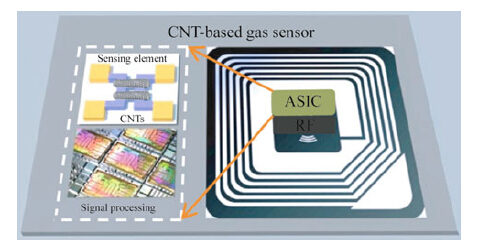 |
| Fig. 1 Conceptual illustration of a complete CNT-based gas sensor using CNTs as sensing elements implemented directly into a MEMS/ CMOS chip with RF circuitry for direct communication with the consumer |
Single crystal silicon microstructures for localized CNT synthesis were designed and fabricated, using the commercial process SOIMUMPs (silicon-on-insulator multi-user MEMS process). Previously, our group has used polysilicon structures in the PolyMUMPS (Polysilicon multi-user MEMSprocess) process [7]. This previous demonstration on polysilicon structures (also used as comparison in the present work) is important as model structures for simulating a process that integrates CNTs on CMOS/ MEMS at low cost. Single crystal structures using silicon-on-insulator (SOI) is a more well-defined test vehicle, eliminating the influence of grain boundaries on conductivity. The process also gives the possibility to design a hole in the chip. Such a hole allows for transmission imaging of CNTs crossing the hole using S(T)EM (scanning electron microscope with transmission imaging option), revealing far more details than SEM (scanning electron microscope) using secondary electron imaging. Both SOIMUMPs and PolyMUMPs use standard microfabrication techniques, as specified in http://www. memscap.com/products/mumps. In both cases, the device layer is doped with phosphorus (n-doping).
Figure 2 shows an example of such a microstructure, with two microbridges. The primary bridge is heated resistively, and is designed with a wider central part for a more uniform temperature distribution, and with a meandering part to account for the thermal expansion occurring during local CNT synthesis.
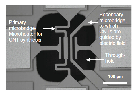 |
| Fig. 2 Micrograph of SOI microstructure for localized CNT growth |
Four different designs were made, microscope images of the resulting designs are shown in Fig. 3. Each has a through-hole for transmission imaging in S(T)EM, and a wider central part (20 lm, as opposed to 10 lm for the supporting beams). Designs 1 and 2 have spring-like beams as described in the previous paragraph. Designs 1 and 3 contain two additional, narrow beams for four-point resistance measurements, thus being a measurement of the temperature of the growth structure. The beams are narrow to minimize the heat leakage and the effect on the microheater temperature. Four-point measurement of the resistance in this part of the structure with fairly uniform temperature gives a far more reliable temperature measurement than the two-point measurement done over the whole microbridge (including supporting beams, wire bonding pads and connections), since the latter method implies integrating over structures with large temperature variations. However, two-point measurement is the preferred method for process control since it requires fewer connections and simpler structures. Comparing two-point and four-point measurements for verification of the twopoint measurement method is therefore important.
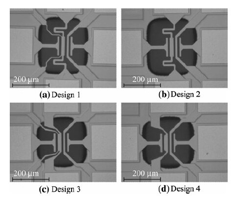 |
| Fig. 3 Four different designs of microstructures |
For SOIMUMPs, the doping concentration at the surface is of the order 1020 cm-3 [15], and decreases with distance down into the device layer (in our case: the microbridges). This doping profile arises from the solid-state dopant diffusion following deposition of a phosphosilicate glass layer and annealing. As comparison, the doping level of PolyMUMPs is more uniform, in the order of 1020 cm-3.
FEM simulations give the relation between the current flowing in a specific microstructure design, and the temperature distribution in the microstructure. The doping profile of the Si structure is modelled as a two-layer structure: an upper, heavily doped 1 lm thick layer and a "bulk" part (the remaining 9 lm thickness of the singlecrystal device layer) with more than four orders of magnitude lower doping concentration. The modelled doping profile is in accordance with the sheet resistance measured in Ref. [15]. The simulation model takes into account the temperature-dependent electrical conductivity of the two modelled Si layers, the temperature-dependent thermal conductivity and thermal expansion, as well as the Thomson effect (charge carriers transporting heat). 2.2 Synthesis and characterization
A thin layer (1-3 nm) of Fe is thermally evaporated on the Si microstructure, to act as catalyst forCNT growth. This is done in a mask-free process. The layer is sufficiently thin to avoid short-circuiting of the structure, and the Fe film forms nanoparticles upon thermal annealing of the primary microbridge [16]. The growth structure is heated in inert atmosphere (Ar) by passing a current through it. At the desired growth temperature, the heated microstructure is exposed to a flow of C2H2 and Ar, while an electric field is applied between the two microstructures in the design. Fig. 4 shows a sketch of the growth process. The current between the two microstructures is monitored during growth, a jump in this current revealing a CNT closing the circuit between the two structures.
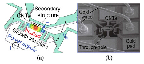 |
| Fig. 4 a Sketch of the CNT growth process. b Micrograph showing electrical connections |
The structures with integrated CNTs are inspected using SEM, both in secondary electron mode, and in transmission imaging mode using a S(T)EM (Hitachi S5500). IV-curves, showing the current flowing in the CNTs connecting the two microbridges as function of the voltage applied between them are measured.
As a preliminary test for the applicability of our approach to fabricate a sensor for monitoring the aging process for food, a system with CNTs connecting microbridges was exposed to alternating CO2 and Ar atmosphere. The resistance of the system was measured in a Wheatstone bridge configuration (the measured signal thus being a voltage signal).
In order to demonstrate the possibility to functionalize our CNTs, thermal evaporation of metals such as Sn and Pd was done on systems with CNTs directly integrated. 3 Results and discussion 3.1 Design
The simulated electrical resistance for the four different microbridge designs are shown in Fig. 5. The shape of the curves reflect the temperature-dependent resistivity of doped silicon: increasing temperature leads to decreasing carrier mobility (hence increased resistivity) due to increasing phonon scattering, until a cross-over where the excitation of electron-hole pairs in intrinsic silicon (density increasing with temperature) gives decreasing resistivity with increasing temperature. The centre temperature of the microbridge during CNT synthesis can be obtained by measuring the resistance, using Fig. 5 as conversion.
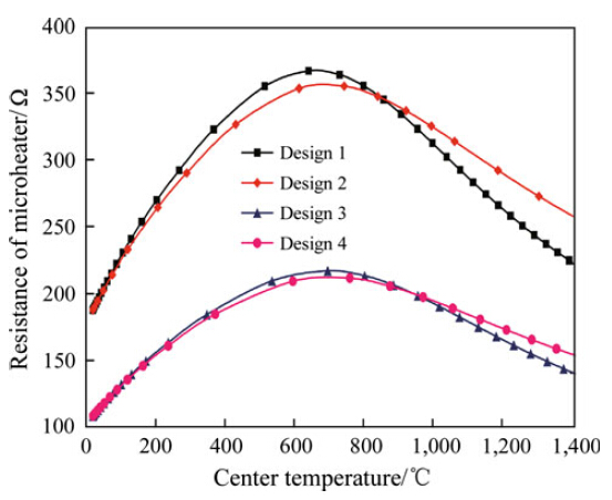 |
| Fig. 5 Simulated resistance of microheaters as function of centre temperature |
To verify the precision of the simulations in Fig. 5, the simulation results are plotted as resistance versus supplied heating power, and compared with experimental values, as shown in Fig. 6. The simulated values are found to represent the experiment well, both for 2-point and four-point measurements. The technique of temperature measurement through resistance measurement, also using the simplified 2-point measurement, is therefore found to be relevant. This implies that a real system can have a simplified design without the additional beams for four-point measurement, and with a reduced number of interconnections.
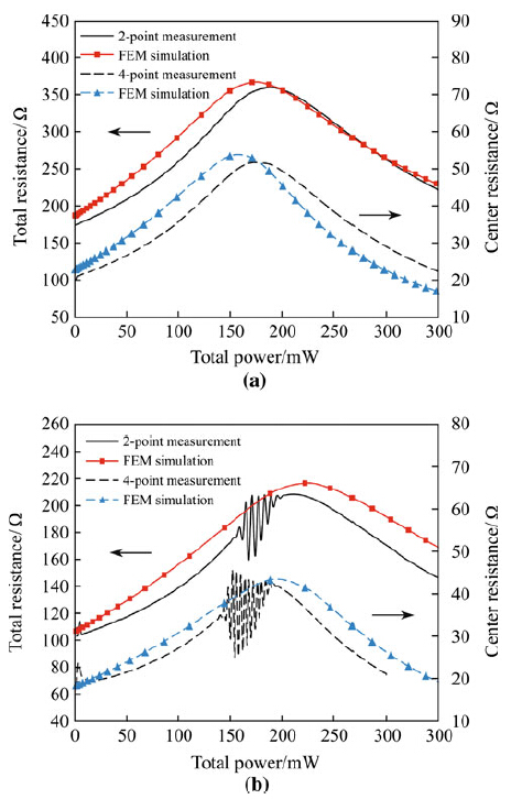 |
| Fig. 6 Measured and simulated resistance of microheaters as function of heating power (2-point measurements represent the entire microbridge, whereas 4-point measurements represent the central part with fairly uniform temperature). a Design 1, b Design 3. The oscillations in the measured curve in b are caused by an artifact of the power control system |
Figure 7 shows the simulated temperature profiles for the four different microheater designs, with a heating power supply corresponding to a maximum temperature of 950 °C. The temperature profile is quite uniform in the region of interest, with a temperature window of 38°C (Design 1) to 106°C (Design 4) for the central, wide part of the microheaters.
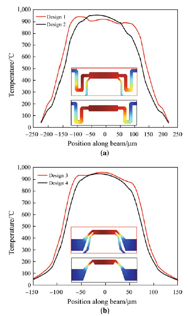 |
| Fig. 7 Simulated temperature profiles for the four microheater designs |
Figure 8 shows a micrograph of a Design 4 microstructure after CNT growth, together with the simulated temperature profile. This is the design with the largest temperature variation (see Fig. 7), and the temperature-dependent variations in CNT growth density can cleary be observed. This underlines the importance of microstructures with a uniform temperature, for predictable and uniform CNT growth. The three other designs, having more uniform temperature distributions, also exhibited a higher uniformity in CNT growth across the microheater.
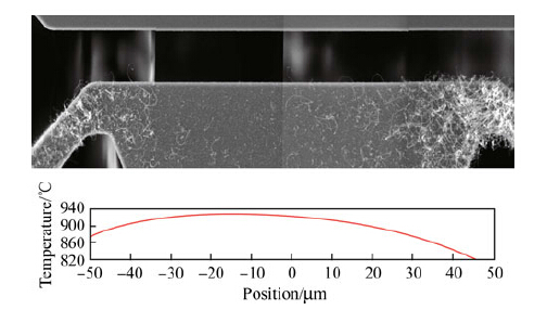 |
| Fig. 8 Microheater (Design 4) after CNT growth with simulated temperature profile |
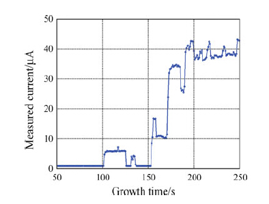
Figure 9 shows an example of the current measured between the two Si microstructures during the synthesis process. Positive steps in the current are observed when CNTs connect the two structures, forming a closed electrical circuit. Negative steps in this current are observed when connections are broken. In the early time of the synthesis process, the connections are somewhat fragile, as shown in Fig. 9.
 |
| Fig. 9 Current flowing in CNT connections during the synthesis process |
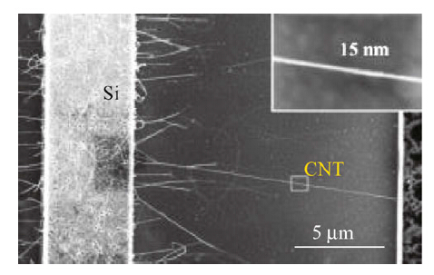
Figure 10 shows a typical image of resulting CNTs from our local synthesis/ direct integration approach (in this case from a poly-Si growth structure). A large number of CNTs grow on the hot microstructures. Whereas most of these grow in a disordered fashion, resulting in curled structures on the Si microbridge, a number of CNTs are straight and actually close the gap between the two microstructures, as expected from the current-time measurement shown in Fig. 9. The CNTs closing the gap are the ones that contribute to an electric circuit, and the ones that are of importance for e.g. sensing applications. A detailed statistical analysis, supported by an electrostatic and thermodynamic model, shows that the thinner CNTs (d < 5-10 nm) are straight and aligned to the electric field, whereas CNTs with higher diameters tend to be more disordered [17]. The local growth process in itself is not expected to produce as well-ordered CNTs as a bulk process with possibilities of subsequent refining. However, this diameter-dependence on field alignment effectively ensures that the thin, straight CNTs are the ones that become part of a Si-CNT based device.
 |
| Fig. 10 CNTs grown on heated poly-Si microstructure |
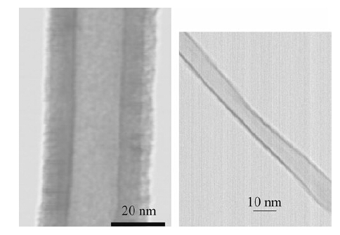
Figure 11 shows high-magnification transmission images of individual CNTs, with diameters about 40 nm and 8 nm, respectively. Three different contrasts appear (best seen in the 40 nm CNT), easily interpreted as a multi-walled CNT (MWCNT) with inner diameter given by the width of the bright core in the image, and the multi-wall thickness given by the width of the dark contrast. The outermost semi-bright feature may be disordered carbon deposits.
 |
| Fig. 11 Detailed view of individual CNTs, transmission image in S(T)EM |
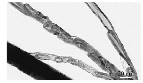
The CNTs produced in our method have a significant variation in degree of order. The micrograph in Fig. 12 shows an example of CNTs with high defect density. Such CNTs are observed when the synthesis temperature is lower than optimal [18].
 |
| Fig. 12 CNTs showing defect structures, transmission image in |
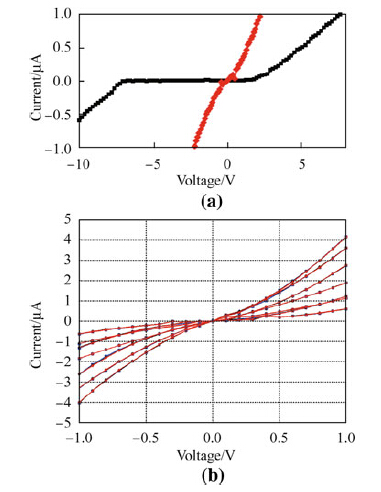
IV-curves (see Fig. 13) show that the Si-CNT-Si system can have both rectifying and near-ohmic behaviour. Systems on the SOIMUMPs platform (see Fig. 13a) show either a rectifying (Schottky-like) or a near-ohmic behaviour, whereas the systems on the PolyMUMPs platform (see Fig. 13b) show a more ohmic behaviour. These platforms differ in their doping level: the PolyMUMPs has a uniform, high, doping level whereas the SOIMUMPs has a decreasing doping level with depth in the device layer. CNTs can grow from different depth locations at the primary microbridge, and connect to different locations at the secondary microbridge. We assume our CNTs to be multiwalled (as suggested by their diameters), hence metallic. Connecting to highly doped Si, an ohmic behaviour is expected, as shown in Fig. 13b. For lower doping levels at the junction, a Schottky-type metal-to-semiconductor junction is created. The circuit can then be modelled as two diodes connected back-to-back in series with a resistance [19]. An applied voltage higher than the reverse breakdown voltage of one of the diodes is needed for a current to flow in either direction. The near-ohmic behaviour observed for several structures, is interpreted as a connection between MWCNT and intermediately highly doped Si. Note that the deviations from linear, ohmic behaviour always result in slightly "S-shaped" curves, qualitatively resembling the shape of the Schottky-type curve of Fig. 13a. In order to achieve true ohmic behaviour, higher doping levels for the Si structures should be used.
 |
| Fig. 13 IV-curves for Si-CNT-Si systems (a) SOIMUMPs microstructure, giving near-ohmic or rectifying (Schottky-like) behaviour. b PolyMUMPs microstructure, giving near-ohmic behaviour. Note that the IV- scales are orders of magnitude different in (a) and (b). |
A demonstration of the capability of CNTs directly integrated in Si microsystems to act as a gas sensor is presented in Ref. [20], where we show that the Si-CNT-Si system changes resistance significantly whether the system is exposed to Ar or CO2. The ability to differentiate Ar to CO2 is relevant for monitoring of aging of food, since many food products are packaged in inert atmosphere, and CO2 is a typical product of a fermentation process. A more detailed work on the sensitivity of the method is ongoing.
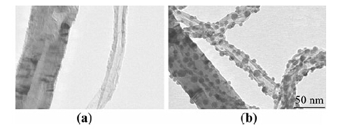
The sensitivity and selectivity to various gases can be enhanced through functionalization of CNTs. Fig. 14 shows one of our early results in functionalization with tin oxide nanoparticles, using the approach of thermal evaporation of Sn. This is a straightforward experimental approach that does not expose the chip to high temperatures. Tin oxide is a relevant functionalization material, sensitive to several gases such as NOx, CO, O2, H2 and NH3. Similarly, we have functionalized our CNTs with Pd nanoparticles [21] using thermal evaporation, Pd typically being used for the detection of H2. As observed in Fig. 14, the tin oxide nanoparticles appear to be uniform in size and distribution along the CNT.
 |
| Fig. 14 a A CNT before thermal evaporation of Sn. b A CNT covered with tin oxide nanoparticles after thermal evaporation. Transmission images in S(T)EM |
A defect-free CNT does not necessarily bond well to foreign elements. Defects in a CNT represent sites where chemical bonds may be made, and may act as nucleation sites for functionalization agents. The distribution of defects shown in our CNTs (Fig. 12 shows an example with very high defect density), may therefore be to our benefit.
A detailed study of the effect of functionalization, using various materials and different processes, is in progress. 4 Conclusions
The presented method has great potential as a last process step to give nano-functionality to processed CMOS/ MEMS wafers. It is controlled by electrical measurements alone, and can thus easily be automated and scaled to wafer-level. CNTs can be used in their virgin state, or they can be functionalized to increase the sensitivity and selectivity to various gases and analytes. Such a system may for instance be used as a sensor for ageing of food.
The designs presented in this paper show a good uniformity in temperature of the growth structure (variations down to 38°C). We demonstrate that the simplified twopoint resistance measurement corresponds to a good temperature measurement, comparable to the inherently more precise four-point measurement of the central part of the growth structure.
Both ohmic contacts, as well as Schottky junction contacts, can be obtained, and very straight CNTs connecting the two microstructures can be manufactured.
Acknowledgements The Research Council of Norway is acknowledged for grants to support the NORFAB infrastructure.| 1. | Kawano T, Chiamori HC, Suter M, Zhou Q, Sosnowchik BD, Lin L (2007) An electrothermal carbon nanotube gas sensor. Nano Lett 7:3686-3690 |
| 2. | Jacobs CB, Peairs MJ, Venton BJ (2010) Review: carbon nanotube based electrochemical sensors for biomolecules. Anal Chim Acta 662:105-127 |
| 3. | Avouris P, Freitag M, Perebeinos V (2008) Carbon-nanotube photonics and optoelectronics. Nat Photonics 2:341-350 |
| 4. | Zhang T, Mubeen S, Myung NV, Deshusses MA (2008) Recent progress in carbon nanotube-based gas sensors. Nanotechnology 19(33):332001 |
| 5. | Morris JE, Iniewski K (eds) (2013) Nanoelectronic device applications handbook. CRC Press, Boca Raton, FL, USA |
| 6. | Martel R, Schmidt T, Shea HR, Hertel T, Avouris P (1998) Single- and multi-wall carbon nanotube field-effect transistors. Appl Phys Lett 73:2447-2449 |
| 7. | Aasmundtveit KE, Ta BQ, Lin LW, Halvorsen E, Hoivik N (2012) Direct integration of carbon nanotubes in Si microstructures. J Micromech Microeng 22(7):074006 |
| 8. | Aasmundtveit KE, Ta BQ, Hoivik N, Halvorsen E (2013) Electrical control on synthesis conditions for locally grown CNTs on polysilicon microstructures. In: Morris JE, Iniewski K (eds) Nanoelectronic Device Applications Handbook. CRC Press, Boca Raton, FL, USA |
| 9. | Qingqing G, Albert E, Fabel B, Abdellah A, Lugli P, Chan-Park MB, Scarpa G (2011) Solution-processable random carbon nanotube networks for thin-film transistors. In: 11th IEEE conference on nanotechnology, IEEE-NANO, pp 378-381 |
| 10. | Cullinan MA, Culpepper ML (2011) Design and fabrication of single chirality carbon nanotube-based sensors. In: 11th IEEE conference on nanotechnology, IEEE-NANO, pp 26-29 |
| 11. | Englander O, Christensen D, Lin L (2003) Local synthesis of silicon nanowires and carbon nanotubes on microbridges. Appl Phys Lett 82:4797-4799 |
| 12. | Christensen D, Englander O, Jongbaeg K, Lin L (2003) Room temperature local synthesis of carbon nanotubes. In: Third IEEE conference on IEEE-NANO, pp 581-584 |
| 13. | Dittmer S, Nerushev OA, Campbell EEB (2006) Low ambient temperature CVD growth of carbon nanotubes. Appl Phys A Mater Sci Process 84:243-246 |
| 14. | Ta BQ, Hoivik N, Halvorsen E, Aasmundtveit KE (2011) Electrical control of synthesis conditions for locally grown CNTs on polysilicon microstructure. In: 11th IEEE conference on nanotechnology, IEEE-NANO, pp 374-377 |
| 15. | Miller DC, Boyce BL, Dugger MT, Buchheit TE, Gall K (2007) Characteristics of a commercially available silicon-on-insulator MEMS material. Sens Actuators A Phys 138:130-144 |
| 16. | Nguyen QH (2012) Catalyst Preparation for local synthesis of carbon nanotubes. Dissertation, Vestfold University College |
| 17. | Ta BQ, Halvorsen E, Hoivik N, Aasmundtveit KE (2013) Diameter dependency for the electric-field-assisted growth of CNTs. Appl Phys Lett (accepted) |
| 18. | Ta BQ, Haugen TB, Hoivik N, Halvorsen E, Aasmundtveit KE (2013) Local synthesis of CNTs in Si microsystems: the effect of temperature distribution on growth structure.Materials 6:3160-3170 |
| 19. | Haugen TB, Ta BQ, Halvorsen E, Hoivik N, Aasmundtveit KE (2013) Integration of CNTs in microsystems: local growth and electrical properties of contacts. Materials 6:3094-3107 |
| 20. | Nguyen QH, Ta BQ, Hoivik N, Halvorsen E, Aasmundtveit KE (2013) CNT-based gas sensor for expiration detection of perishable food. In: 13th IEEE conference on nanotechnology, IEEENano, Beijing, China, pp 675-678 |
| 21. | Ta BQ, Ngo AV, Nguyen QH, Hoivik N, Halvorsen E, Aasmundtveit KE (2013) Deposition of Pd on suspended and locally grown CNTs using thermal evaporation. In: 13th IEEE conference on nanotechnology, IEEE-Nano, pp 1176-1179 |
 2013, Vol. 1


